
PCB Fiducials: The Essential Guide to Design & Placement

Table of Content
- 1. Why Fiducials Are Critical for PCB Assembly?
- 2. What Are Fiducial Marks on a PCB?
- 3. Types of Fiducial Marks
- 4. Key Design Rules and IPC Standards
- 5. Strategic Placement for Optimal Performance
- 6. The Indispensable Role of PCB Fiducials in SMT Assembly
- 7. Common PCB Fiducial Design and Placement Mistakes to Avoid
- 8. PCB Fiducials FAQs
- 9. Summary
- Key Takeaways
1. Why Fiducials Are Critical for PCB Assembly?
In the intricate world of Printed Circuit Board(PCB) manufacturing, precision is paramount. Every component, no matter how tiny, must be placed with absolute accuracy to ensure the functionality and reliability of the final product. This is where fiducials come into play. Often overlooked by the uninitiated, these small, distinctive copper patterns are indispensable reference points that guide automated assembly equipment, ensuring components are placed correctly and efficiently. Without properly designed and strategically placed fiducial marks, the entire Surface Mount Technology(SMT) assembly process would be significantly compromised, leading to increased defect rates, production delays, and higher costs.
This comprehensive guide dives deep into the world of PCB fiducials, exploring their types, the crucial design rules, and best practices for their placement. Whether you’re a seasoned PCB designer, a hardware engineer, or simply curious about the nuances of electronic manufacturing, understanding fiducials is key to developing high-density, high-reliability products that meet the rigorous demands of modern electronics. We’ll cover everything from IPC standards to practical tips, ensuring you have the knowledge to optimize your PCB designs for seamless assembly and inspection.
2. What Are Fiducial Marks on a PCB?

Fiducial marks are precisely defined reference points, typically circular copper pads, etched onto a PCB. Their primary function is to provide accurate alignment and positional data for automated manufacturing equipment, such as pick-and-place machines, solder paste printers, and automated optical inspection(AOI) systems. These machines use optical recognition systems to ‘see’ and locate fiducials, allowing them to precisely determine the PCB’s orientation, scale, and exact position on the assembly line.
Think of them as GPS coordinates for your PCB. Just as a GPS helps you navigate, fiducials guide robotic equipment to perform highly accurate tasks. By correcting for any X-Y offset, rotation, or scaling inaccuracies that might occur when the board is loaded onto the machine, fiducials enable precise solder paste deposition and component placement, especially critical for fine-pitch components like BGAs(Ball Grid Arrays) and QFNs(Quad Flat No-leads).
The composition of a fiducial mark generally includes two parts: the marking point(the copper pad itself) and a surrounding clearance area(solder mask opening). This contrast allows the optical systems to easily identify and lock onto the fiducial, even in varying lighting conditions.
3. Types of Fiducial Marks

Fiducials are categorized based on their application and placement strategy on the PCB. Understanding the differences between these types is crucial for effective PCB design and placement.
1) Global Fiducial Marks
Global fiducials are used for the overall alignment of the entire PCB. They provide a common reference point for all features on the board. For the most accurate positional information, a minimum of three global fiducials should be placed on each PCB. This three-point system allows the assembly equipment to correct for any X-Y translation and rotation of the entire board. It’s generally recommended that these fiducials be placed in a non-symmetrical pattern to prevent ambiguity in orientation detection. Ideally, they are located on the same side of the board as the components that will be mounted.
According to IPC guidelines, global fiducials should be located on all PCB layers that contain components to be mounted with automated equipment. A common strategy suggests placing the lower-left fiducial at the(0,0) datum point, with the other two in the positive X and Y directions.
2) Local Fiducial Marks
While global fiducials handle overall board alignment, local fiducials are essential for precise alignment of specific, critical components. These are typically placed near fine-pitch components such as BGAs, QFNs, and other integrated circuits(ICs) where extreme placement accuracy is required. Local fiducials help compensate for localized distortions or manufacturing tolerances that might not be fully addressed by global fiducials alone. A pair of local fiducials(at least two) is usually sufficient for aligning an individual component, providing localized X-Y and rotational data.
Their proximity to the component minimizes the impact of any slight material expansion or contraction across the board, ensuring that solder paste is printed and components are placed exactly where they need to be, significantly improving yields for challenging placements.
3) Panel Fiducial Marks
When multiple PCBs are fabricated together on a larger panel(a process known as panelization or array creation), panel fiducials are used. These marks are placed on the tooling strip or “breakaway rail” of the panel, not on the individual boards themselves. They serve to align the entire panel within the assembly machine. Once the panel has been processed, these rails and the panel fiducials are typically discarded when individual PCBs are separated. Panel fiducials accommodate the clamping edges of pick-and-place machines and ensure accurate recognition across the entire manufacturing array.
4. Key Design Rules and IPC Standards
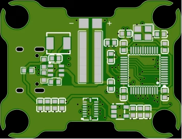
Adhering to established design rules and IPC standards is paramount for creating effective fiducial marks. IPC-7351(Generic Requirements for Surface Mount Design and Land Pattern Standard) provides comprehensive guidelines for fiducial design.
1) Standard Dimensions
The standard shape for a fiducial mark is a solid, non-plated copper circle. Key dimensions include:
- Diameter:Typically 1.0mm(0.040 inches) to 3.0mm(0.120 inches). A common recommended diameter is 1.0mm.
- Solder Mask Clearance:A concentric clearance area of solder mask opening around the copper pad is crucial. This non-solder masked area should be at least equal to the diameter of the copper pad itself. So, if the copper pad is 1.0mm, the clearance should extend at least 1.0mm beyond the pad’s edge, creating an overall diameter of at least 3.0mm(1mm pad + 1mm clearance on each side). This contrast is vital for machine vision systems.
- Surface Finish:Fiducial marks should have the same surface finish as the component pads on the PCB, typically ENIG(Electroless Nickel Immersion Gold) or OSP(Organic Solderability Preservative), to ensure consistent optical properties and prevent reflection issues.
Here’s a table summarizing typical fiducial design parameters:
| Parameter | Recommended Specification(IPC-7351) | Purpose/Benefit |
| Fiducial Shape | Solid Non-Plated Copper Circle | Clear optical recognition, cost-effective |
| Fiducial Diameter | 1.0mm(0.040 in) to 3.0mm(0.120 in) | Optimal machine vision detection |
| Solder Mask Clearance(Annular Ring) | Equal to fiducial diameter(min) | Creates contrast for optical systems |
| Surface Finish | Same as component pads(e.g., ENIG, OSP) | Consistent optical properties, prevents reflections |
| Material | Bare copper with surface finish | Standard material, good contrast |
2) Fiducial Material and Construction
Fiducials should be made of bare copper, covered with the same surface finish as the rest of the board’s pads. They must be free of solder mask on the pad itself and within the clearance area. This design creates a clear contrast between the reflective copper pad and the matte solder mask, enabling reliable optical detection.
5. Strategic Placement for Optimal Performance
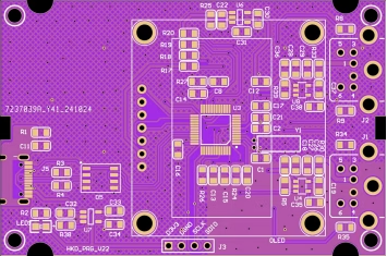
The placement of fiducials is as critical as their design. Incorrect placement can negate their benefits, leading to assembly issues.
1) Quantity and Distribution
- Global Fiducials:A minimum of three global fiducials is recommended for each side of the PCB where SMT components are placed. They should be distributed as far apart as possible from each other and located near the edges of the board. This maximizes the reference area and helps compensate for board dimensional variations.
- Local Fiducials:For fine-pitch components, at least two local fiducials should be placed diagonally opposite each other(e.g., upper-left and lower-right) for the component. Placing them within 1-5mm of the component’s pad array is ideal.
2) Distance to the Edge
Fiducials should be placed a suitable distance from the board edge to avoid being obscured by tooling rails or clamps. A common recommendation is to place the center of the fiducial at least 3.85mm(0.150 inches) from the edge of the PCB. This ensures they are clear of any manufacturing tooling or handling areas, especially important for panel fiducial marks on breakaway rails.
3) Avoid Symmetrical Placement
For global fiducials, symmetrical placement(e.g., in a perfect square) should be avoided. A non-symmetrical, L-shaped or triangular arrangement is preferred. If only two fiducials are placed symmetrically, the assembly machine might struggle to determine the correct orientation of the board, leading to incorrect component placement.
4) Clearance from Other Features
Ensure that fiducials are free from any other copper features, silkscreen, drill holes, or legend printing that could interfere with the vision system. The clearance area around the fiducial should be completely clear to maintain optical integrity.
6. The Indispensable Role of PCB Fiducials in SMT Assembly
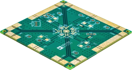
Fiducials are not merely helpful; they are a core manufacturing requirement for modern SMT assembly, especially with the increasing density and miniaturization of electronic components. Their critical functions include:
- Pick-and-Place Accuracy:Automated pick-and-place machines use fiducials to accurately position components onto their designated pads. Before placing each component, the machine takes an image of the fiducials, calculates any offsets, and adjusts its placement coordinates. This is vital for fine-pitch parts where a fraction of a millimeter misalignment can cause bridging or open circuits.
- Solder Paste Registration:Before components are placed, solder paste is applied to the pads. Solder paste printers also utilize fiducials to align the stencil perfectly with the PCB. Accurate solder paste deposition is the foundation of reliable SMT joints; misregistration leads to soldering defects.
- Automated Optical Inspection(AOI):After solder paste printing and component placement, AOI machines use fiducials to precisely locate and inspect solder joints and component positions. They compare the actual image to the ideal CAD data, identifying defects like missing components, incorrect orientation, or poor solder joints.
- Yield Improvement:By ensuring precise alignment throughout the assembly process, fiducials dramatically reduce defect rates. For complex boards with BGAs and QFNs, which are highly susceptible to placement errors, fiducials are the difference between high yields and costly rework or scrap.
7. Common PCB Fiducial Design and Placement Mistakes to Avoid
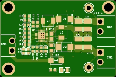
Even with clear guidelines, mistakes can happen. Here are some common pitfalls in fiducial design and placement:
- Insufficient Clearance:Not providing enough solder mask clearance around the copper pad can reduce the contrast needed by vision systems, making reliable detection difficult.
- Symmetrical Placement:Placing only two global fiducials in a perfectly symmetrical arrangement can confuse the machine about the board’s orientation. Always opt for a non-symmetrical, three-point setup.
- Obstructed Fiducials:Allowing silkscreen, component outlines, test points, or other copper features to overlap with or obscure fiducials or their clearance areas.
- Incorrect Surface Finish:Using a different surface finish for fiducials than for component pads can lead to inconsistent reflectivity and optical recognition issues.
- Too Few Fiducials:Relying only on global fiducials for highly dense boards with many fine-pitch components. Local fiducials are critical for these specific parts.
- Placing Fiducials on the Wrong Layer:Fiducials must be placed on the component layer for the automated equipment to use them. For double-sided assembly, fiducials are needed on both top and bottom layers.
- Placing on a Board Section That Will Be Separated:If a board is panelized and will be broken apart, global fiducials should be on the final board or panel fiducials on the rail, not on a section that gets discarded.
By understanding and avoiding these common errors, designers can ensure their PCB design is optimized for manufacturing, leading to a smoother assembly process and higher quality products.
8. PCB Fiducials FAQs
Question1: Are fiducials always necessary for PCB assembly?
For automated SMT assembly, especially with fine-pitch components, fiducials are mandatory. While manual assembly might not strictly require them, almost all modern production lines rely on them for accuracy and efficiency.
Question2: Can I use more than three global fiducials?
Yes, you can. While three is the minimum for full X-Y and rotational correction, having more(e.g., four, one in each corner) can sometimes offer additional robustness against board warping or measurement errors. However, ensure they are still strategically placed and non-symmetrical for orientation.
Question3: What happens if my fiducials are not correctly designed or placed?
Incorrect fiducials can lead to a host of problems including misaligned solder paste, inaccurate component placement, increased rework, higher scrap rates, and delays in production. For dense or fine-pitch designs, it can make automated assembly virtually impossible.
Question4: Can I use through-hole pads as fiducials?
While theoretically possible, it’s generally not recommended. Solid, non-plated copper pads provide a more consistent and reliable optical target for machine vision systems, especially with varying plating thicknesses or hole tolerances.
Question5: Should fiducials have a specific surface finish?
Yes, the surface finish over the fiducial mark is crucial. It needs to be sufficiently reflective for machine vision but not so shiny that it causes glare. Common finishes like OSP(Organic Solderability Preservative), ENIG(Electroless Nickel Immersion Gold), or Immersion Tin are typically suitable.
9. Summary
Fiducial marks are tiny but mighty elements in PCB design, serving as critical optical reference points for automated manufacturing equipment. This guide has illuminated their indispensable role in ensuring precise SMT assembly, from accurate solder paste printing to flawless component placement and robust inspection. We’ve explored the different types—global fiducial for overall board alignment, local fiducial for fine-pitch components, and panel fiducial for panelized arrays—each vital for specific alignment tasks. Adhering to strict IPC standards for design, including specified diameters, solder mask clearance, and surface finishes, is crucial. Furthermore, strategic placement, emphasizing a non-symmetrical three-point system for global fiducials and close proximity for local ones, significantly enhances assembly yields. By understanding these principles and avoiding common mistakes, PCB designers can optimize their layouts for manufacturing efficiency and product reliability, ensuring a smoother journey from design to a fully functional electronic device.
Key Takeaways
- Fiducials are Mandatory:Essential for automated PCB assembly equipment(pick-and-place, solder paste printers, AOI) to ensure precision.
- Three Types Exist:Global(for entire board), Local(for fine-pitch components), and Panel(for arrays).
- Ad here to IPC Standards:Follow IPC-7351 guidelines for fiducial dimensions(e.g., 1.0mm copper pad, 1.0mm concentric clearance).
- Strategic Placement is Key: Use a non-symmetrical, three-point pattern for global fiducials; place local fiducials close to critical components.
- Avoid Common Mistakes:Ensure ample clearance, non-symmetrical arrangement, correct layer placement, and consistent surface finish to prevent assembly issues.








