
OrinewPCB · PCB fabrication + turnkey assembly
Controlled Impedance PCB Manufacturing
Bring your high-speed or RF design from an impedance requirement to a clear manufacturing plan—and, when needed, a complete assembled board.
Send OrinewPCB your PCB files, target impedance and proposed stackup. Include a BOM and placement file for one inquiry covering PCB fabrication, component sourcing and turnkey PCB assembly.
Not ready for assembly? Tell us you need bare PCBs only. Stackup changes, achievable tolerance and testing scope are confirmed for your project before production.
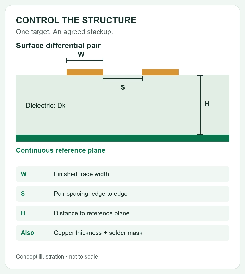
What is a controlled impedance PCB? It is a PCB whose specified signal traces are manufactured to an agreed characteristic impedance and tolerance. The result depends on the trace geometry, dielectric properties and reference-plane arrangement—not simply the board’s layer count or nominal copper weight.
Start with the interface requirement
When Does PCB Impedance Control Matter?
RF transmission lines and digital interfaces with fast signal edges can be sensitive to impedance discontinuities. Clock frequency alone is not enough to decide: trace length, edge rate, routing transitions and the interface’s loss and timing budgets also matter.
| Signal example | Typical requirement to discuss | Confirm in your design files |
|---|---|---|
| RF signal path | A 50Ω single-ended transmission line is common in RF systems. | Device and connector requirements, line structure, operating band and permitted loss. |
| USB differential pair | 90Ω differential is specified in many USB layout guides. | The exact USB interface and device guidance, tolerance, reference plane and routing constraints. |
| Ethernet differential pair | 100Ω differential is common for specified PHY-to-magnetics pairs. | PHY layout guidance, interface segment, magnetics and any local plane or isolation constraints. |
| Other high-speed interface | Use the target required by the actual interface and device. | Single-ended versus differential requirements, net classes, layers and acceptance criteria. |
Use your device vendor’s current layout guide and interface requirements to set the target and tolerance. A 90Ω differential pair does not automatically mean two independent 45Ω traces; pair coupling changes the relationship.
Confirm before releasing fabrication files
An Impedance Target Needs a Manufacturable Stackup
A trace width copied from another board may give a different impedance on your stackup. Agree the finished structure with the fabricator, then check the layout against it. Wider or thicker copper is not automatically better for high-speed signals.
Width, spacing and reference planes
Define the controlled layer and reference plane, finished trace width and copper thickness. Differential structures also need pair spacing. Include relevant solder-mask assumptions for surface traces.
Dielectric thickness and properties
Specify dielectric thickness and the material’s appropriate design Dk. FR-4 is not one fixed electrical value. Material selection should consider frequency, loss budget, processing and availability; lower Dk alone is not a quality ranking.
Keep changes visible
State whether trace-width, spacing or stackup changes are permitted. Request approval before controlled geometry or materials change. If the stackup changes, recalculate the impedance and review the affected routing.
For RF material requirements, see our Rogers PCB manufacturing information. If the laminate is not fixed, send the operating band and loss requirement with your inquiry rather than specifying only “high-frequency PCB.”
A clear engineering handoff
From Impedance Requirements to Production
Use these six checkpoints to keep engineering, purchasing and production working from the same revision.
Submit the requirement
Identify controlled net classes, layers, target values, tolerances, quantity and board revision. Flag requirements that are still open.
Confirm stackup and geometry
Review materials, dielectric thicknesses, finished copper and width/spacing assumptions. Resolve proposed adjustments before manufacturing release.
Agree verification
Define coupon structures, measurement method, sampling scope, reporting and acceptance limits. Specify any actual-board measurement requirement separately.
Approve the build package
Align the fabrication notes, Gerber or ODB++ package and approved stackup. For assembly, align the BOM, placement data and assembly drawing too.
Fabricate and assemble to scope
Quote bare-board manufacturing or a turnkey build. Confirm component substitutions, assembly inspection and product testing before proceeding.
Review records and revisions
Request the agreed manufacturing records. Keep impedance results separate from functional acceptance and document changes before the next batch.
Understand what the test proves
Impedance Coupons, TDR and PCBA Verification
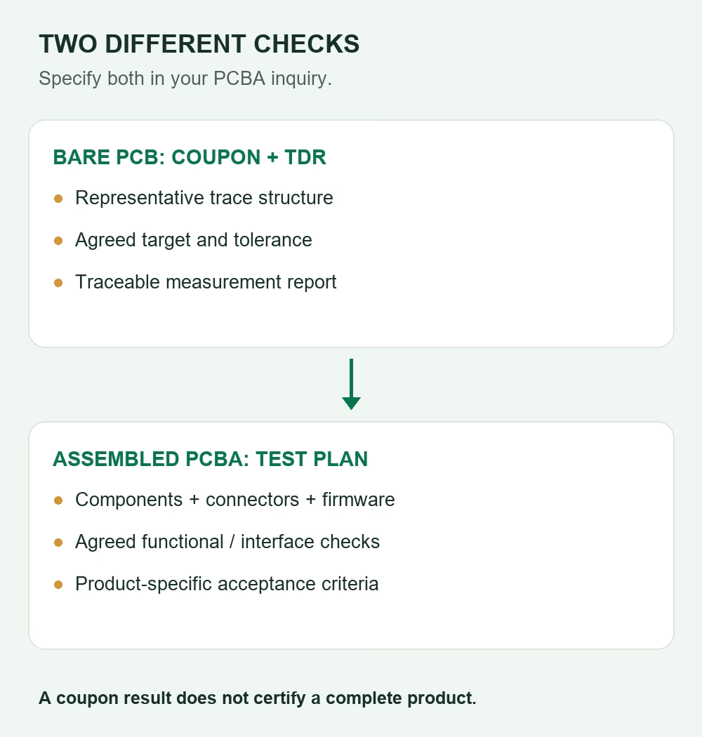
Time-domain reflectometry (TDR) is commonly used to check controlled impedance. A representative test coupon is fabricated with the panel and reproduces the relevant layer, conductor and dielectric structure. Coupon design, probing and the chosen measurement region affect how the result is interpreted.
A passing coupon supports verification of the agreed manufacturing structure. It does not by itself prove every routed path, connector transition, via stub or assembled interface meets the product’s complete signal-integrity requirements.
- For the bare PCB: agree target, tolerance, coupon coverage, measurement and traceability.
- For the assembled product: define power-up, firmware, interface or other functional tests and supply the necessary procedure, fixtures and pass/fail criteria.
- For detailed signal performance: specify any eye-diagram, loss or S-parameter evaluation separately. These are not implied by a standard assembly inquiry.
Tell us what evidence your engineering or quality team needs so its feasibility and scope can be reviewed in the quotation.
One inquiry, a defined build scope
Need Controlled Impedance Boards and Turnkey PCB Assembly?
A high-speed board’s fabrication requirements belong in the same release package as its components and assembly instructions. Ask OrinewPCB to review the complete build so PCB changes, BOM decisions and test requirements can be coordinated.
PCB + components + assembly
Send fabrication files, impedance notes, BOM, placement data and assembly drawing. Specify programming and testing needs for a project-specific quotation.
Bare controlled impedance boards
Request PCB-only manufacturing if your assembly supply chain is already arranged. Include the approved stackup and impedance verification requirements.
Specify parts and substitution rules
Provide manufacturer part numbers, quantities and approved alternatives. Flag constrained RF, interface and timing parts; substitutions require your approval.
Explore the OrinewPCB brand’s turnkey assembly service. Required processes, inspection, test scope and delivery plans are confirmed against the submitted project.
Prepare a useful quotation request
What to Send for a Controlled Impedance PCB Quote
Start with the files you have. Mark missing or provisional requirements so we can identify the next information needed before the build is released.
| Item | PCB-only inquiry | Add for turnkey PCB assembly |
|---|---|---|
| Design package | Gerber or ODB++, drill files, fabrication drawing and revision. | Matching assembly drawing and pick-and-place/centroid data. |
| Impedance table | Net class, controlled layer, reference plane, single-ended/differential target and tolerance. | Identify the assembled interface and any product-specific acceptance test. |
| Stackup and materials | Layer arrangement, board thickness, laminate requirements, finished copper and solder-mask assumptions. | Flag component or connector constraints that could be affected by PCB changes. |
| Verification | Coupon requirements, TDR scope, sampling, report and traceability needs. | Inspection, programming and functional testing procedures; fixture ownership and pass/fail limits. |
| Parts | Not required for bare-board-only manufacturing. | BOM with manufacturer part numbers, quantities, approved alternatives and supplied-part details. |
| Commercial scope | Prototype and production quantities, destination and requested schedule. | Full or partial turnkey scope, build quantities, release milestones and packaging requirements. |
Example of a Clear RFQ Note
“Please quote PCB fabrication, component sourcing and assembly for revision C. The attached impedance table identifies the USB pair and RF nets, target values, tolerances and layers. Please propose a compatible stackup for approval, identify any required width/spacing changes, and confirm coupon/TDR reporting. BOM, placement file and assembly drawing are attached. Programming and functional-test requirements are listed separately.”
Illustrative wording only; use your actual interface requirements and approved tolerances. Do not copy a target from this example into a released design without engineering review.
For a more complete assembly handoff, use our PCB assembly drawing guide and prototype-to-production PCB assembly checklist.
Controlled Impedance PCB FAQs
What is the difference between single-ended and differential impedance?
Single-ended impedance describes a signal conductor relative to its reference structure. Differential impedance describes the pair driven with opposite signals. It depends on both individual trace geometry and coupling between the traces. Specify which value applies to each net class.
Can you quote PCB fabrication and turnkey assembly together?
Yes. Request PCB fabrication, BOM sourcing and assembly in the same inquiry. Send the impedance requirements with the fabrication files, then add the BOM, placement file and assembly drawing. Programming and testing should be specified as separate, explicit parts of the requested scope.
Can I request controlled impedance without a final stackup?
You can submit an inquiry with a proposed or incomplete stackup. Include target values, tolerances, layer count, material constraints and any fixed geometry. The manufacturable structure and permitted changes need approval before production; an inquiry is not an engineering release.
What impedance tolerance is available?
The achievable tolerance must be reviewed for the actual materials, geometry, manufacturing process and measurement method. State the tolerance your design needs rather than assuming a standard percentage. Confirm it in the quotation and approved fabrication requirements.
Does every high-speed PCB need Rogers material?
No. Choose materials using the interface or RF design requirements, operating band, loss budget and manufacturability. FR-4 and specialist laminates have different properties, and a material’s design Dk and loss characteristics should be appropriate to the calculation and application.
Will a passing impedance coupon guarantee my USB or Ethernet link works?
No. A representative coupon checks an agreed PCB manufacturing structure. Complete interface performance also depends on routing discontinuities, connectors, vias, components and the assembled system. Define functional or signal-integrity acceptance checks separately.
Can you source components or assemble customer-supplied parts?
Discuss full or partial turnkey sourcing in your inquiry. Provide manufacturer part numbers, quantities and approved alternatives. For customer-supplied parts, include packing, labeling and handling information. Part availability and any substitutions are confirmed for the project.
How do I avoid surprises when moving from prototype to production?
Release one aligned revision of the stackup, impedance table, PCB fabrication data, BOM and assembly instructions. Document approved changes, verification requirements and test criteria. Revisit impedance assumptions when materials, layer construction or controlled geometry change.
Ready to review your build?
Turn Your Impedance Requirement into a Complete PCBA Inquiry
Send the PCB package and impedance notes. Add your BOM and assembly files if you need a complete turnkey build. Tell us what is fixed, what can change and what must be verified.
PCB-only and component-sourcing inquiries are welcome too. Project feasibility, inspection, pricing and schedule are confirmed after review.
[email protected]
Contact the OrinewPCB Team
Include quantity, revision and requested delivery destination so the team can assess the complete scope.
