
PCB Assembly Drawing: A Practical Guide for Turnkey PCBA
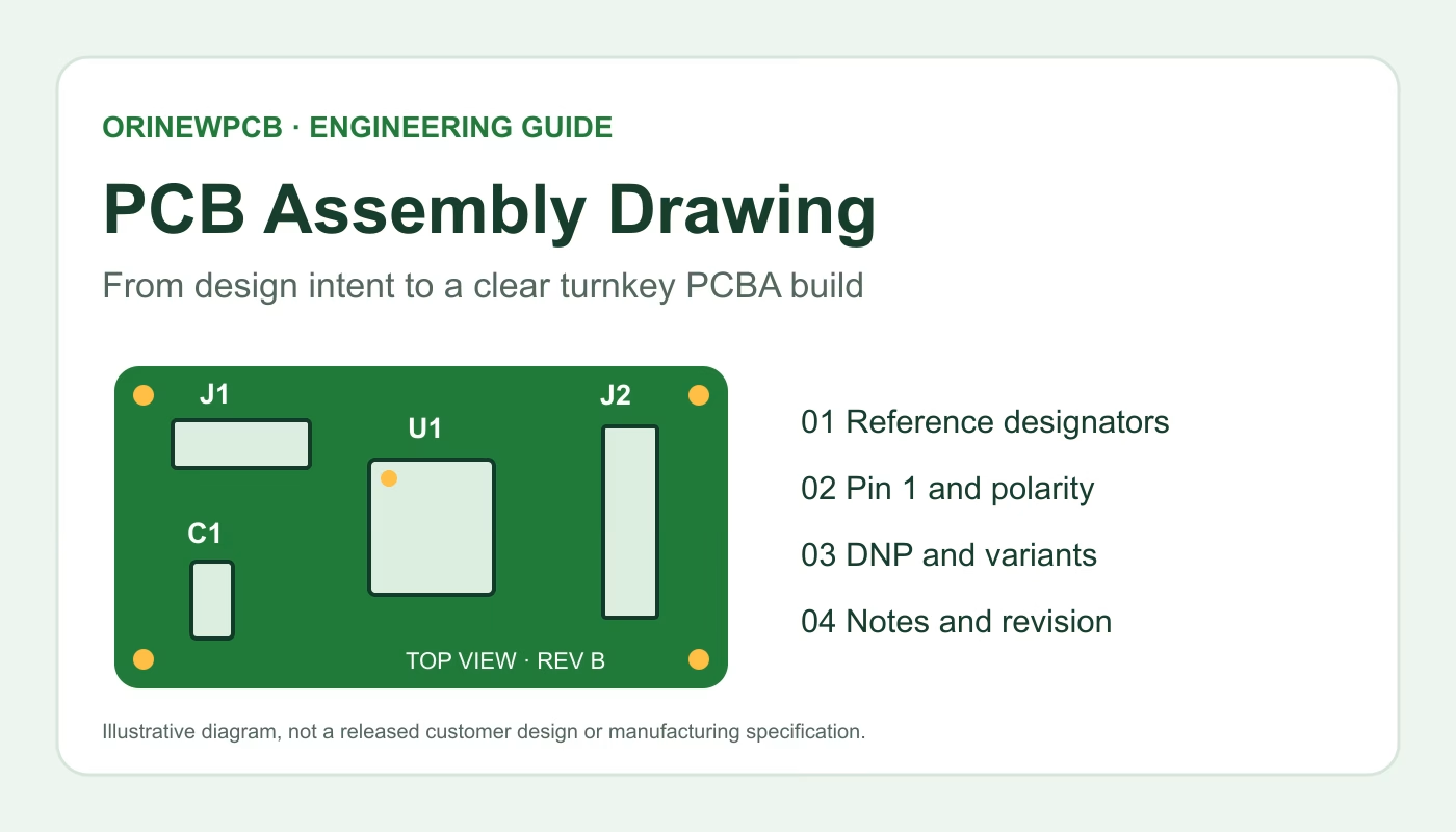
Table of Content
ORINEWPCB · DESIGN HANDOFF & TURNKEY PCBA
A PCB assembly drawing tells an assembler how to populate and finish a circuit board. It should make board identity, top and bottom views, reference designators, polarity, pin 1, do-not-populate (DNP) positions and special assembly instructions clear. Release it with a matching bill of materials (BOM) and component placement file.
For a turnkey PCB assembly inquiry, the drawing helps connect your engineering intent to component sourcing, placement, secondary assembly and the agreed test scope. This guide gives hardware engineers a practical drawing checklist, product managers a release workflow, and buyers a way to identify quotation gaps.
What a PCB assembly drawing does
A useful drawing removes ambiguity at the point where a CAD design becomes a build instruction. The assembler needs to know which component belongs at each reference, which side it belongs on and which operations are required after placement. Connector orientation, polarized parts, hardware, wires and variants deserve particular attention.
For example, a BOM may identify connector J2 precisely while a placement file supplies its location. The drawing can clarify the mating direction, fitted height or mechanical constraint that matters to the product. Those details should come from the released design and component documentation.
The drawing is also a communication reference during review. A question such as “Is R9 fitted on Variant A?” is easier to resolve when the engineer, sourcing team and assembler refer to the same marked view and revision. It does not replace a review of the other manufacturing files.
Assembly drawing vs. BOM, Gerber and placement files
Each file answers a different question. Treat the release as a coordinated package, rather than expecting one document to communicate everything. Swipe the tables horizontally on a phone.
| Document | Main purpose | Check before sending |
|---|---|---|
| Assembly drawing | Visual placement intent, orientation, variants and assembly notes. | Readable top/bottom views, references, DNP status and revision. |
| BOM | Identifies the parts to procure or supply for each fitted position. | Exact manufacturer part numbers, quantities, references and approved alternatives. |
| Placement / CPL file | Machine-readable component position, rotation and board side. | Units, origin, reference-point convention, bottom-side convention and export filters. |
| Gerber + drill data | Defines the PCB layer artwork and drilling information. | Matching board revision, complete required layers, drills and outline. |
| Fabrication drawing | Defines bare-board specifications and requirements. | Stack-up, thickness, materials, finish, tolerances and other design requirements. |
| Programming / test instructions | Defines firmware loading and agreed verification. | Version, equipment, access, limits, records and responsibilities. |
An integrated data format may carry fabrication and assembly information together. Confirm the assembler’s accepted format and the additional instructions still needed. For a project quotation, our turnkey assembly scope guide explains how fabrication, sourcing and assembly fit into one request.
The PCB assembly drawing checklist
1. Identify the board, document and build variant
Include the board or assembly part number, drawing number, revision, date, sheet number and variant name. Use meaningful identifiers that match the rest of the release package. If the assembly revision and bare-board revision differ, state their approved relationship explicitly.
Label the status of an early drawing as provisional or for quotation when appropriate. A product manager should be able to distinguish the package used for budgeting from the package authorized for production.
2. Show the relevant board views clearly
Provide separate top and bottom views when both sides contain fitted parts. Label the viewing direction and ensure the bottom view cannot be confused with a transparent top view. Show the board outline and enough recognizable features to orient the reader.
Use detail or side views where the normal plan view cannot explain a connector, bracket, height constraint or wire attachment. State critical dimensions from the design; do not ask the operator to infer them from print scale.
3. Make reference designators and orientation readable
Every fitted component should be traceable to its BOM reference. Keep labels out of crowded outlines where possible, and use enlarged details for dense areas. Check the PDF at normal reading size, not just while zoomed in inside the CAD tool.
For polarized parts and ICs, communicate the relevant orientation or pin 1 information. Cross-check component markings against the actual manufacturer part number and datasheet. A body stripe or dot is not a universal polarity convention across all component types.
4. Define DNP parts and variants consistently
DNP means a component position is intentionally not populated for a specific build. Mark it on the drawing and in the BOM or controlled variant list. Confirm whether the placement export excludes DNP parts or includes them with an agreed status field.
If two product variants use the same PCB, release variant-specific instructions instead of relying on a verbal note. A component alternative also needs approval; it should not become a different variant accidentally.
5. Specify secondary assembly and mechanical details
Identify through-hole connectors, leads, jumpers, wires, brackets, heatsinks, adhesive or other operations when required. Provide installation direction, material and relevant limits. Confirm these details when reviewing through-hole PCB assembly or mixed-technology work.
For coating or cleaning requirements, define the specified process, keep-outs and acceptance criteria in the relevant drawing or linked instruction. If a connector must remain accessible for programming or testing, make the process sequence clear.
6. Reference the agreed programming and acceptance instructions
Identify the test procedure and firmware release by document or file reference. Define required inspections, functional checks, fixtures and result records in the RFQ. An assembly drawing does not itself establish functional performance or certify the finished product.
If an acceptance standard is specified, identify its document, revision and class, plus customer-specific requirements. Ask the supplier to confirm the quoted scope; special testing, programming or fixture development should be explicit.
PCB assembly drawing example: five details to review
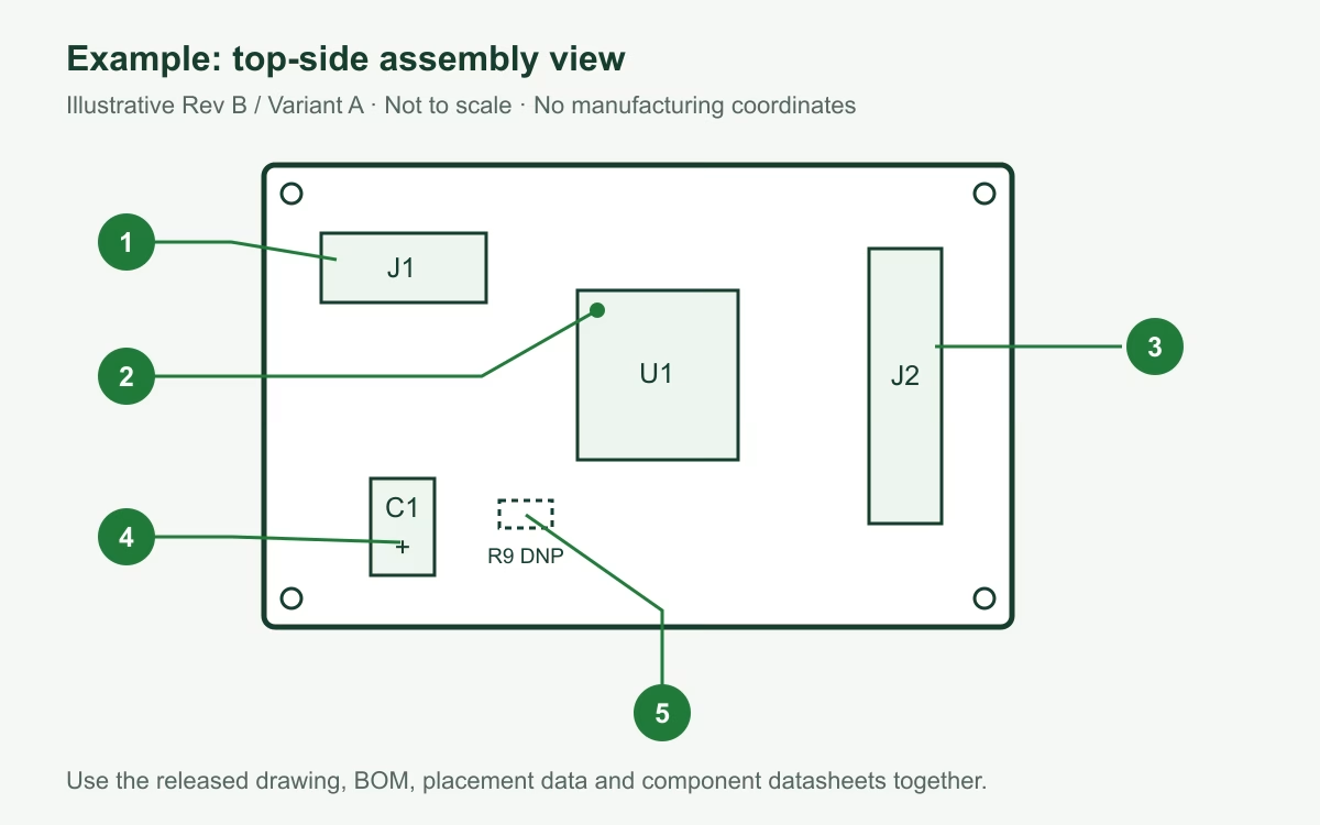
- J1 reference: the label connects the visual position to the corresponding BOM line.
- U1 pin 1: the marked corner makes the intended orientation visible; the actual part documentation must confirm it.
- J2 connector: the view shows a placement position, but an application may also need mating-direction and height details.
- C1 polarity: the example uses a positive terminal callout. The released drawing should identify the real part’s required polarity.
- R9 DNP: the position is deliberately unpopulated in the illustrated variant and should agree with the variant BOM.
Consider a review finding: the drawing says “R9 DNP,” but the BOM orders one R9 per board and the placement export includes it. Stop and resolve that conflict through a controlled revision or approved clarification. The assembler should not guess which file wins.
| Reference | Illustrative drawing intent | Release check |
|---|---|---|
| J1 / J2 | Install the specified connectors. | Exact part number and fitted quantity match the BOM; direction and height are clear. |
| U1 | Fit the selected IC with pin 1 at the marked corner. | BOM package, footprint and placement orientation refer to the same approved device. |
| C1 | Fit the specified polarized capacitor. | Drawing polarity and the actual component marking are consistent. |
| R9 | Do not populate on Variant A. | DNP status agrees across drawing, BOM/variant list and placement-export handling. |
How to create and verify the drawing
- Freeze the intended revision. Confirm the board layout, BOM and variant definition before generating release outputs.
- Generate views from the CAD project. Use assembly or fabrication-layer views with the relevant outlines, references and orientation information. Remove visual clutter that does not communicate build requirements.
- Add the missing instructions. Include document identity, special operations, details and references to test or programming instructions.
- Export a readable document. PDF is practical for review when accepted by your assembler. Keep the original CAD project under your own release control.
- Compare the exports. Check drawing references and fitted quantities against the BOM and placement file. Review at least the polarized parts, ICs, connectors, DNP positions and non-standard operations.
- Obtain approval and package the release. Record which package was reviewed and accepted, and keep later changes distinguishable from that release.
Altium Designer: assembly outputs and Draftsman board assembly views can produce the visual documentation. Review the selected side, component display and variant before export. Placement export configuration separately controls coordinates, units and included components.
KiCad: select the relevant documentation layers when plotting or printing; F.Fab and B.Fab can show component information and DNP indications according to export settings. Placement export separately controls units, origin and DNP handling. Verify the actual outputs for the version and settings you use.
Rotation and bottom-side conventions can differ between exports and assembly workflows. Document the convention and ask the assembler to confirm it during data review. Do not manually reverse bottom-side coordinates based on an assumed universal rule.
Common file conflicts that delay a turnkey PCBA build
| Problem | Why it matters | Action before release |
|---|---|---|
| Mixed revisions | Procurement and placement may follow different designs. | Regenerate and identify a matching approved package. |
| Ambiguous pin 1 or polarity | The fitted part may face the wrong direction. | Check the actual component documentation and add an unambiguous callout. |
| DNP disagreement | A variant may be populated incorrectly. | Align the drawing, BOM/variant list and placement-file handling. |
| Units or origin not stated | Placement coordinates may be interpreted incorrectly. | State units and export origin, then confirm the assembly interpretation. |
| Missing mechanical details | A correctly soldered connector or heatsink may not fit the product. | Provide detail views and design dimensions where required. |
| Test scope left open | Quotations may exclude fixtures, programming or needed verification. | Define procedure, equipment, acceptance and reporting in the RFQ. |
Use the prototype-to-production checklist for the wider release process. To compare quotations on equal scope, see our turnkey PCB assembly cost breakdown.
Watch: what to send for a PCB and PCBA quotation
In this official OrinewPCB video, the five quotation inputs include PCB manufacturing data, board specifications, quantity, a clean BOM, and assembly or testing information. Use it as a short overview alongside the drawing checks above.
Watch this video on YouTube · OrinewPCB official channel
Video: “How to Get a Fast, Accurate PCB Quote | 5 Things to Send,” OrinewPCB, published October 9, 2026. The quoted project scope and schedule still require a review of your actual requirements.
Prepare one release package for your RFQ
A clear folder structure helps the recipient identify what is current. The names below are examples, not mandatory formats:
Controller_RevB_VariantA_RFQ/
  01_PCB_Fabrication_RevB/
  02_BOM_RevB_VariantA.xlsx
  03_Placement_RevB_VariantA.csv
  04_Assembly_Drawing_RevB_VariantA.pdf
  05_Programming_and_Test_Requirements.pdf
  06_RFQ_Quantity_Date_Destination.txt
Hardware engineer: approve the file consistency, orientation, variant and technical instructions. Product manager: identify sample and batch quantities, open decisions, target date and release owner. Buyer or business owner: confirm sourcing responsibility and compare complete quoted scope, rather than assembly price alone.
For full turnkey, specify PCB fabrication, BOM sourcing and assembly together. If you supply selected components, identify those BOM lines and use the partial turnkey sourcing checklist. You can also review one-stop PCB assembly on the OrinewPCB brand website and learn about OrinewPCB.
PCB assembly drawing FAQ
What is a PCB assembly drawing?
A PCB assembly drawing is a visual instruction document for populating and finishing a circuit board. It identifies components, orientation, DNP positions, special assembly notes and the released board revision. It is used with the BOM and placement data.
Is a PCB assembly drawing the same as a fabrication drawing?
No. The assembly drawing explains component installation and related operations. The fabrication drawing specifies the bare PCB. They should identify the same board revision and reference compatible manufacturing data.
Can Gerber files replace the assembly drawing?
Gerber data describes PCB layers; it does not by itself communicate every assembly decision, variant or special operation. Send a matching BOM, placement data and drawing, or confirm an accepted integrated manufacturing-data package with the assembler.
Does every component need a coordinate in the assembly drawing?
The visual drawing does not have to repeat the entire coordinate list. Placement files provide machine-readable positions. The drawing should resolve orientation, side, special locations and assembly requirements that cannot be inferred safely from the placement file alone.
How should I mark do-not-populate parts?
State the build variant and mark DNP components consistently in the drawing and BOM or approved variant list. Confirm how DNP records are handled in the placement export. Do not depend on a missing BOM row as the only instruction.
Can I use a PCB screenshot as an assembly drawing?
A screenshot can help explain a question, but a released drawing should remain readable and include board identity, revision, view side, component references, orientation and relevant notes. Verify the exported document independently of the CAD editor.
Do turnkey PCBA quotations automatically include firmware and functional testing?
Do not assume they do. Describe firmware, programming access, fixtures, test procedure and acceptance limits in the RFQ. Confirm the scope, tooling, price and timing for your project.
Can I request an OrinewPCB quote before the drawing is final?
Yes. You can discuss a prototype or planned batch using the available PCB files, BOM and requirements. Mark incomplete or provisional items clearly. Production release should use a confirmed revision and agreed assembly and test instructions.
Request a turnkey PCB assembly quote
Send OrinewPCB your Gerber or agreed PCB fabrication data, BOM, placement file and assembly drawing. Include prototype or production quantities, target date, destination and programming or test requirements. Clearly flag provisional files and pending decisions.
Copy this inquiry outline: “Please quote full turnkey PCB fabrication, BOM sourcing and assembly for [board/revision/variant], [prototype quantity] and [planned batch quantity]. Assembly drawing and placement data are attached. Firmware/test requirements are [available/pending]. Target date and destination: [details]. Please flag file conflicts, unavailable parts and any scope exclusions.”
Files are optional for the initial discussion and can follow by email at [email protected]. Final price, available scope and schedule follow project review.
Related Posts



ORINEWPCB · PROJECT SUPPORT
Contact Us
Discuss your PCB assembly project with our team.
FREE QUOTE
Plan your turnkey PCBA build.
Share your quantity and requirements. Add Gerber files and a BOM when ready.
Files are optional for an initial discussion. Include any assembly, sourcing or testing requirements in your message.




