High Frequency PCB
Table of Content
- Specify the RF requirements that affect fabrication
- Keep RF material changes under engineering control
- Every bare PCB receives flying-probe electrical testing
- From bare boards to genuine-component turnkey PCBA
- Nine PCBA quality stages with an agreed test scope
- Plan delivery from the complete release package
- Request a High Frequency PCB review
- High Frequency PCB questions
ORINEWPCB · FABRICATION TO TURNKEY ASSEMBLY
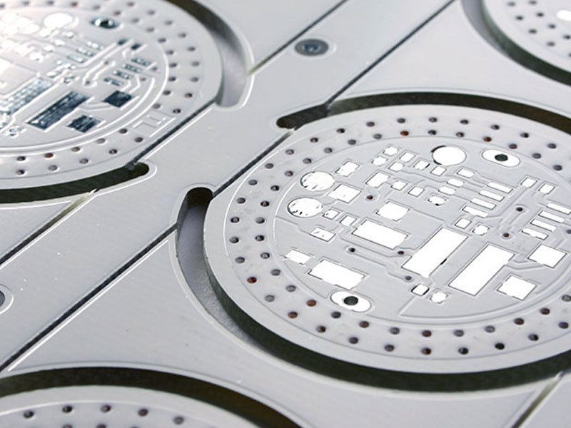
A high frequency PCB needs a material and stack-up selected for the circuit’s operating band and loss budget. Specify the laminate grade, design dielectric data, copper and impedance requirements together. Flying-probe testing of the bare board does not establish RF insertion loss or assembled radio performance.
Specify the RF requirements that affect fabrication
Frequency alone is not a complete material specification. Dielectric constant and dissipation factor depend on the material, test method and frequency; copper roughness, geometry and dielectric thickness also influence performance. Review the actual circuit constraints instead of assuming that every RF board should use the same laminate.
On a small screen, swipe the table horizontally. Keyboard users can focus the table region and use the arrow keys.
| Decision | Send or confirm | Why it matters |
|---|---|---|
| Material identity | Required manufacturer/grade and whether substitutions are permitted. | Approve a proposed alternative against the electrical, mechanical and processing requirements. |
| Design dielectric data | Dk/Df basis, operating band, layer construction and critical dielectric thicknesses. | Datasheet values from different methods are not automatically interchangeable design values. |
| Controlled impedance | Net classes, target impedance, tolerance, reference layers and evidence required. | Agree the stack-up and measurement scope before the design is released. |
| Copper and finish | Copper construction/roughness needs and the required surface finish. | Review these against loss, soldering and assembly requirements. |
| RF assembly and test | Connector interfaces, sensitive components, shielding and the planned test procedure. | Define any RF functional test, equipment and pass/fail limits separately. |
Keep RF material changes under engineering control
If the specified material is unavailable or affects the requested date, a fast substitution can create a larger engineering problem. Ask for the proposed grade, construction and technical differences before approving it. For a hybrid stack, identify which layers use which materials and the intended electrical references.
- Provide the fabrication package, operating band and critical RF paths.
- List controlled-impedance requirements and any coupon or report needs.
- Identify the approved material and whether an engineering review of alternatives is acceptable.
- For turnkey assembly, include BOM, placement, connector and shielding instructions.
- Define RF validation separately from bare-board continuity and short-circuit checks.
Every bare PCB receives flying-probe electrical testing
OrinewPCB flying-probe tests every bare PCB we manufacture, not just a sample. This checks the conductive networks against the electrical test data. Include your netlist where available and identify any required test parameters or records in the RFQ.
An electrical pass does not establish every physical characteristic, controlled impedance, RF performance, thermal reliability or finished-product function. Specify those requirements and any additional evidence separately. This keeps the acceptance scope clear before fabrication begins.
From bare boards to genuine-component turnkey PCBA
Keep the fabrication, BOM purchasing and assembly review connected when you need a finished assembly. Small-to-medium batches and high-mix turnkey PCB assembly are a particular OrinewPCB strength. List quantities and differences for each design or variant so the release is unambiguous.
We supply and use 100% brand-new, original, genuine electronic components for customers’ turnkey assemblies. Our cooperation with manufacturers and distributors helps us seek competitive BOM pricing and practical lead times. Exact MPNs, current availability, permitted sources and delivery dates are checked for your project; alternatives require customer approval.
Bare PCB supply
Release the fabrication data, quantity, acceptance scope and delivery needs.
BOM sourcing
Send full manufacturer part numbers, quantities, approved alternatives and documentation needs.
One-stop assembly
Combine fabrication, sourcing, assembly and the agreed inspection or test plan.
Explore one-stop PCB assembly, electronic component sourcing and the OrinewPCB brand website.
Nine PCBA quality stages with an agreed test scope
When the order includes assembly, our quality workflow covers nine stages. The applicable inspection plan and evidence are agreed for the actual build:
- IQC: incoming materials.
- SPI: solder paste inspection.
- Online AOI: in-line optical inspection.
- SMI: first-article inspection.
- IPQC: in-process quality checks.
- Offline AOI: post-solder optical inspection.
- X-ray: hidden joints to the agreed scope.
- Manual QC: workmanship review.
- Pre-shipment QA: identification, quantity and packaging.
These are nine quality stages, not nine functional tests. Programming, ICT, functional testing or application-specific validation need an agreed procedure, access or fixtures, and pass/fail criteria. See our factory and quality workflow.
Plan delivery from the complete release package
We work toward the earliest practical delivery for the approved scope. Send the required quantity, design variants and target date, and state whether it means production completion, dispatch or arrival. Materials, engineering questions, assembly preparation and agreed tests all affect the confirmed schedule.
Compare quotations using the same material, revision, sourcing responsibility and acceptance scope. A lower bare-board or placement line item is not automatically a lower complete project cost.
Related planning: Controlled impedance PCB · HDI construction review · Prototype board evaluation.
Request a High Frequency PCB review
Send OrinewPCB your files and tell us what you need: bare boards, BOM sourcing or a complete turnkey assembly. Files are optional for an initial discussion.
- Board files, drawing revision and special material or construction requirements
- Quantity per design or variant and repeat-order expectations
- BOM with full MPNs, placement and assembly drawings if assembly is needed
- Inspection, programming, functional-test and documentation requirements
- Target date, delivery destination and any staged shipment needs
For direct email: [email protected]. A quote request does not authorize purchasing, substitutions or production.
High Frequency PCB questions
Is high frequency PCB material always PTFE?
No. RF laminate families use different material systems and offer different electrical and processing properties. Select a specific grade for your requirements rather than treating “high frequency” as one chemistry.
Does a flying-probe pass confirm impedance or insertion loss?
No. Specify impedance measurement and any RF performance verification separately, including the method, applicable nets or coupons and acceptance limits.
Can OrinewPCB quote fabrication and RF assembly together?
Yes. Share the board package, approved BOM, placement data and assembly instructions. Any RF test must have an agreed setup, procedure and limits; it should not be assumed from the assembly quote.
Related Posts
ORINEWPCB · PROJECT SUPPORT
Contact Us
Discuss your PCB assembly project with our team.
FREE QUOTE
Plan your turnkey PCBA build.
Share your quantity and requirements. Add Gerber files and a BOM when ready.
Files are optional for an initial discussion. Include any assembly, sourcing or testing requirements in your message.