SMT Stencil
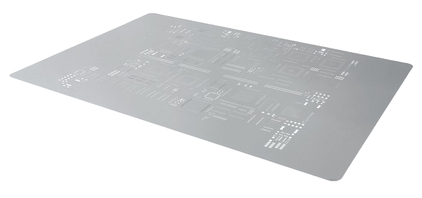
Table of Content
- Match the stencil to the package and printing process
- Use aperture calculations as a review tool
- Coordinate stencil preparation with genuine-component PCBA
- Nine PCBA quality stages with an agreed test scope
- Plan delivery from the complete release package
- Request a stencil and turnkey assembly review
- SMT Stencil questions
ORINEWPCB · FABRICATION TO TURNKEY ASSEMBLY
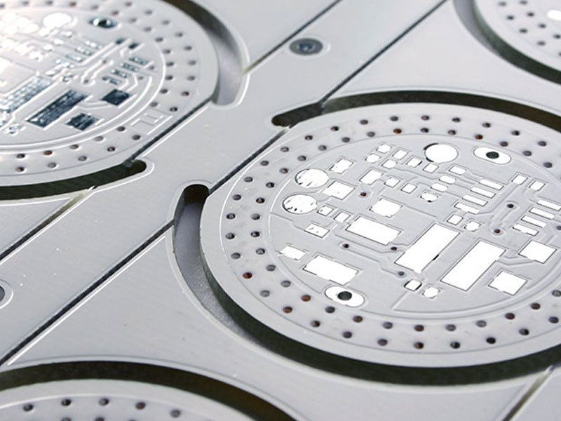
An SMT solder paste stencil meters paste onto PCB pads before component placement. A useful stencil RFQ includes the paste-layer data, board/panel reference, foil requirements and printer or frame interface. Aperture design must match the component and printing process; copying every copper pad at 1:1 is not a universal rule.
Match the stencil to the package and printing process
Foil thickness, aperture shape and aperture wall area affect paste release and deposited volume. Fine-pitch parts and large thermal pads can need different printing considerations on the same board. Package-manufacturer guidance is a starting point; the assembled board and actual print process still need review.
On a small screen, swipe the table horizontally. Keyboard users can focus the table region and use the arrow keys.
| Decision | Send or confirm | Why it matters |
|---|---|---|
| Paste-layer data | Top/bottom paste layers, board outline and revision reference. | Avoid manufacturing from an obsolete paste file or assuming copper artwork is the paste design. |
| Foil and apertures | Requested thickness, smallest apertures and package-specific recommendations. | Review paste release and deposited volume together; one thickness is not ideal for every design. |
| Frame or printer interface | Framed/frameless format, external dimensions, tooling and tension requirements. | The stencil must fit the actual printer or manual setup. |
| Fiducials and panel | Panel drawing, alignment features, rails and board orientation. | Panel changes can invalidate an earlier stencil even when the circuit is unchanged. |
| Mixed package needs | Fine-pitch devices, thermal pads and components requiring special attention. | Discuss whether aperture adjustments or another process approach needs evaluation. |
Use aperture calculations as a review tool
Area ratio compares the aperture opening area with the aperture wall area. For a rectangular aperture, the geometric ratio is L × W / [2 × (L + W) × T], using the same units for length, width and foil thickness. Reducing thickness increases that geometric ratio but also changes paste volume. This is not a universal pass/fail rule or a substitute for package guidance and print validation.
- Send the released paste layers and the matching PCB/panel drawing.
- Identify the component packages that drive the smallest apertures or greatest paste needs.
- Provide printer/frame details and any established process restrictions.
- Approve aperture edits against package guidance and assembly requirements.
- Review actual printing results and any agreed solder paste inspection before continuing the build.
Coordinate stencil preparation with genuine-component PCBA
For a turnkey build, the stencil should refer to the same approved panel and revision as the fabrication and placement files. Small-to-medium batches and high-mix turnkey assembly are a particular OrinewPCB strength. Separate the requirements and quantity for each variant.
We supply and use 100% brand-new, original, genuine electronic components in our customers’ turnkey assemblies. Manufacturer and distributor cooperation helps us seek competitive BOM prices and practical lead times. Exact MPN availability, sourcing requirements and delivery are reviewed for the quote; substitutes need your approval.
A stencil is not an electrical board and is not flying-probe tested. Separately, every bare PCB we manufacture receives flying-probe electrical testing. Board tests, stencil inspection and assembled-circuit testing have different purposes.
Explore one-stop PCB assembly, component sourcing and the OrinewPCB brand website.
Nine PCBA quality stages with an agreed test scope
When the order includes assembly, our quality workflow covers nine stages. The applicable inspection plan and evidence are agreed for the actual build:
- IQC: incoming materials.
- SPI: solder paste inspection.
- Online AOI: in-line optical inspection.
- SMI: first-article inspection.
- IPQC: in-process quality checks.
- Offline AOI: post-solder optical inspection.
- X-ray: hidden joints to the agreed scope.
- Manual QC: workmanship review.
- Pre-shipment QA: identification, quantity and packaging.
These are nine quality stages, not nine functional tests. Programming, ICT, functional testing or application-specific validation need an agreed procedure, access or fixtures, and pass/fail criteria. See our factory and quality workflow.
Plan delivery from the complete release package
We work toward the earliest practical delivery for the approved scope. Send the required quantity, design variants and target date, and state whether it means production completion, dispatch or arrival. Materials, engineering questions, assembly preparation and agreed tests all affect the confirmed schedule.
Compare quotations using the same material, revision, sourcing responsibility and acceptance scope. A lower bare-board or placement line item is not automatically a lower complete project cost.
Related planning: Double-sided PCB fabrication · Prototype assembly planning · One-stop PCB assembly.
Request a stencil and turnkey assembly review
Send OrinewPCB your files and tell us what you need: stencil tooling, bare boards, BOM sourcing or a complete turnkey assembly. Files are optional for an initial discussion.
- Board files, drawing revision and special material or construction requirements
- Quantity per design or variant and repeat-order expectations
- BOM with full MPNs, placement and assembly drawings if assembly is needed
- Inspection, programming, functional-test and documentation requirements
- Target date, delivery destination and any staged shipment needs
For direct email: [email protected]. A quote request does not authorize purchasing, substitutions or production.
SMT Stencil questions
Should stencil apertures always match copper pads exactly?
No. Aperture geometry depends on package guidance, paste requirements, stencil thickness and the printing process. Thermal pads and fine-pitch components may need specific treatment.
Is there one ideal stencil thickness for all components?
No. Thickness affects paste volume and release. Review the whole component mix, the smallest apertures and the required solder deposits before selecting it.
Are SMT stencils flying-probe tested?
No. A solder paste stencil is tooling rather than an electrical PCB. Its dimensions, apertures and fit require appropriate inspection. Our policy of flying-probe testing every bare PCB applies to the boards we manufacture.
Can you manage the stencil as part of turnkey assembly?
Yes. Include the matching board files, BOM, placement and assembly instructions. Stencil preparation, paste printing and applicable inspection can then be reviewed with the complete assembly scope.
Related Posts
ORINEWPCB · PROJECT SUPPORT
Contact Us
Discuss your PCB assembly project with our team.
FREE QUOTE
Plan your turnkey PCBA build.
Share your quantity and requirements. Add Gerber files and a BOM when ready.
Files are optional for an initial discussion. Include any assembly, sourcing or testing requirements in your message.