
Micro-Hole Tech: Tiny Keys to Powerful HDI PCB

Table of Content
- 1. Understanding High Density Interconnect(HDI) PCBs
- 2. What is Micro-Hole Technology?
- 3. Why Micro-Holes are Crucial for Modern Electronics?
- 4. The Manufacturing Process: Laser Drilling Micro-Holes
- 5. Architecture and Types of Micro-Holes in HDI PCBs
- 6. Applications Driving the Need for Micro-Hole Technology
- 7. Advantages and Challenges of Micro-Hole Technology
- 8. The Future of Micro-Hole Technology
- 9. Micro-Hole HDI PCB FAQs
- 10. Summary
- Key Takeaways
In today’s rapidly evolving electronics landscape, the relentless demand for smaller, faster, and more powerful devices has pushed the boundaries of traditional circuit board manufacturing. From the sleekest smartphones to life-saving medical implants and advanced avionics, the need to pack more functionality into increasingly compact spaces is paramount. This drive for miniaturization is precisely where High Density Interconnect(HDI) Printed Circuit Boards(PCBs) and, more specifically, micro-hole technology, emerge as critical enablers.
Micro-hole technology is not just an incremental improvement; it’s a revolutionary advancement that allows for the creation of extremely small holes in PCB substrates, opening up new possibilities for complex circuit designs and enhanced performance. This article delves into the intricacies of micro-hole technology, its symbiotic relationship with HDI PCBs, and how it is shaping the future of advanced electronics.
1. Understanding High Density Interconnect(HDI) PCBs
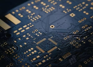
Before diving deep into micro-hole technology, it’s essential to grasp the foundation it builds upon: High Density Interconnect(HDI) PCBs. Unlike traditional PCBs that rely on through-hole vias and conventional drilling methods, HDI boards represent a fundamental shift in design and manufacturing. They are characterized by a higher wiring density per unit area, achieved through several key features:
- Finer lines and spaces
- Smaller vias and capture pads
- Higher connection pad density
- Advanced techniques like sequential lamination
HDI PCBs are primarily made of high-performance thin materials, allowing for thin traces packed closely together. This architecture enables designers to create more complex interconnections and accommodate a greater number of components in a smaller footprint, offering more functionality within the same or even a reduced area. This increased circuit density is a cornerstone for modern, feature-rich electronic devices.
2. What is Micro-Hole Technology?
Micro-hole technology is the sophisticated drilling technique that underpins the capabilities of HDI PCBs. It involves creating extremely small holes, often referred to as microvias, in the PCB substrate. These holes are significantly smaller than those produced by traditional mechanical drilling methods.
Typically, the diameter of micro-holes ranges from 50 to 150 micrometers(µm), though advancements are continually pushing these limits even further. This technology is a cornerstone of modern manufacturing, enabling the high density required for advanced electronics by connecting multiple copper layers within the board. The precision and small size of these holes are critical for achieving the high circuit density and enhanced signal integrity characteristic of HDI designs.
3. Why Micro-Holes are Crucial for Modern Electronics?
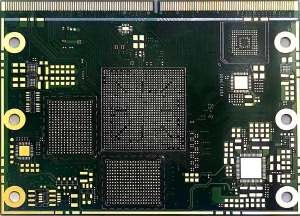
The significance of micro-hole technology extends beyond mere size reduction. It addresses several critical challenges in modern electronics design and manufacturing:
1) Miniaturization: As electronic devices become smaller and more portable, components need to be packed closer together. Micro-holes facilitate this by providing tiny pathways for interconnections, reducing the overall board size and weight. This is vital for products like smartphones, wearables, and compact medical devices.
2) Improved Signal Integrity: Shorter signal paths, made possible by smaller vias and closer component placement, lead to reduced electromagnetic interference(EMI) and better impedance control. This is crucial for high-frequency applications, ensuring faster data transmission and improved performance, especially in high-speed digital circuits and RF applications.
3) Enhanced Reliability: Smaller vias reduce the stress on the PCB material, which can improve the board’s long-term reliability. Additionally, advanced architectures utilizing copper-filled micro-holes offer increased structural integrity and better heat dissipation, particularly important for high-power components.
4) Increased Functionality: By freeing up valuable board space, micro-hole technology allows for more complex circuit designs, additional components, and advanced features, ultimately leading to more capable and versatile electronic products.
The shift towards smaller, more efficient components is a rapid trend across various industries, and micro-hole technology is a key enabler of this transformation.
4. The Manufacturing Process: Laser Drilling Micro-Holes
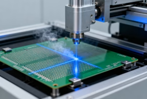
The creation of micro-holes demands precision that traditional mechanical drilling often cannot provide, especially for diameters below 150 µm. Laser drilling is the predominant method used for manufacturing these tiny vias.
Various types of lasers are employed, each suited for different materials and hole characteristics :
- CO2 Lasers:Commonly used for drilling through dielectric materials. They are efficient for creating blind and buried vias in the substrate layers.
- UV Lasers(Nd:YAG, Excimer):These lasers offer extremely high precision and can drill through copper, making them ideal for creating micro-holes directly in pads or for more intricate drilling tasks.
The laser drilling process allows for highly accurate and repeatable results, critical for the dense interconnects found in HDI PCBs. Unlike mechanical drills, lasers do not create mechanical stress or wear, minimizing damage to the delicate PCB structure. The ability to control laser parameters like pulse duration, power, and beam focus allows manufacturers to achieve specific hole geometries and wall qualities.
5. Architecture and Types of Micro-Holes in HDI PCBs
The sophistication of HDI PCBs is further enhanced by the various types of micro-hole architectures that can be implemented:
| Via Type | Description | Benefit |
| Blind Vias | Connect an outer layer to one or more inner layers, but do not pass through the entire board. | Frees up routing space on the opposite side, improving density. |
| Buried Vias | Connect two or more inner layers and are completely enclosed within the PCB, invisible from the outer surfaces. | Maximizes routing density on outer layers and internal layers. |
| Stacked Vias | Micro-holes directly stacked on top of each other across multiple layers. Often copper-filled for reliability. | Enables vertical interconnections through many layers in a compact area. |
| Staggered Vias | Micro-holes offset from each other on different layers. | Offers flexibility in routing when direct stacking is not feasible or desired. |
Many advanced HDI designs utilize multi-layer stacked copper-filled micro-holes. Filling these micro-holes with copper before subsequent lamination steps increases their reliability and mechanical stability, allowing for greater design flexibility and robustness, particularly for fine-pitch components.
6. Applications Driving the Need for Micro-Hole Technology
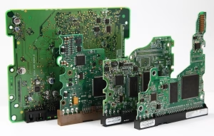
Micro-hole technology in HDI PCBs is not just a theoretical concept; it’s a practical necessity driving innovation across numerous industries. Its impact is evident in:
- Consumer Electronics:Smartphones, tablets, smartwatches, and other wearables heavily rely on HDI PCBs with micro-holes to achieve their compact form factors and high functionality. Devices like 4G/5G communication modules and touch-screen computers benefit immensely.
- Medical Devices:Miniaturized and highly reliable electronics are crucial for medical implants, diagnostic equipment, and portable healthcare devices. HDI with micro-holes enables these life-saving technologies.
- Automotive Electronics:Advanced driver-assistance systems(ADAS), infotainment systems, and engine control units(ECUs) require dense and robust PCBs that can withstand harsh environments while providing complex interconnections.
- Aerospace and Defense:High-reliability, lightweight, and compact electronic systems are paramount for avionics, satellites, and intelligent military equipment, where space and weight savings are critical.
- Industrial IoT and Robotics:As industrial control systems and robots become more intelligent and integrated, the need for dense, reliable, and space-efficient PCBs increases.
The ability of micro-hole technology to enable smaller, lighter, flatter, and more portable products has truly revolutionized the electronics industry, especially as SMT component technology progresses with increasingly finer pitch packaging like flip-chips and chip-level packaging.
7. Advantages and Challenges of Micro-Hole Technology
Advantages:
- Space Efficiency:Significantly reduces PCB size and weight, allowing for more compact product designs.
- Enhanced Electrical Performance:Improves signal integrity, reduces noise, and enables faster data rates, crucial for high-speed circuits.
- Increased Reliability:Copper-filled vias and reduced stress points contribute to longer product lifespans.
- Greater Design Flexibility:Allows for more complex routing, finer pitch components, and advanced component placement strategies.
- Cost-Effective Miniaturization:While initial manufacturing costs can be higher, the ability to shrink products and improve performance can lead to overall cost savings and market advantages.
Challenges:
- Higher Manufacturing Complexity:Requires specialized equipment(laser drills) and expertise, leading to potentially higher production costs and longer lead times compared to conventional PCBs.
- Material Selection:Demands high-performance laminates suitable for laser drilling and fine-line processing.
- Yield Management:Maintaining high yields with such small features requires stringent process control and quality assurance.
- Thermal Management:Higher component density can lead to increased heat generation, necessitating advanced thermal management solutions within the compact design.
Despite these challenges, the benefits offered by micro-hole technology overwhelmingly outweigh the drawbacks for advanced electronic applications, making it an indispensable part of modern PCB manufacturing.
8. The Future of Micro-Hole Technology
The trajectory for micro-hole technology is one of continuous advancement. As demand for even smaller and faster devices grows, we can expect:
- Smaller Via Diameters:Research and development are constantly pushing the limits, with efforts to achieve even finer micro-holes.
- New Laser Technologies:Innovations in laser drilling, potentially involving new wavelengths or pulse regimes, will further enhance precision and efficiency.
- Advanced Materials:Development of new dielectric materials with improved properties suitable for ultra-fine features and high-frequency performance .
- Integration with AI and Automation:Increased use of artificial intelligence in design for manufacturability(DFM) and automated process control to optimize micro-hole fabrication.
Micro-hole technology will remain at the forefront of HDI PCB evolution, continually enabling the next generation of revolutionary electronic devices.
9. Micro-Hole HDI PCB FAQs
Question1: What is the typical size range for micro-holes in HDI PCBs?
Micro-holes typically range in diameter from 50 to 150 micrometers(µm). This is significantly smaller than holes created by traditional mechanical drilling methods.
Question2: What is the primary difference between a micro via and a standard through-hole?
Micro vias are significantly smaller(typically < 150 µm diameter) and usually connect only adjacent layers(blind or buried), unlike standard through-holes which pass through the entire board.
Question3: Why is laser drilling preferred over mechanical drilling for micro-holes?
Laser drilling offers the precision required for such small diameters, minimizes mechanical stress on the delicate PCB materials, and can create holes in various materials including copper and dielectrics, which mechanical drills often struggle with at these sizes.
Question4: What are the main benefits of using micro-hole technology in electronics?
The main benefits include enabling extreme miniaturization, improving signal integrity for faster performance, enhancing the overall reliability of the circuit board, and allowing for increased functionality within a smaller device footprint.
Question5: Are all micro holes filled?
Not all micro holes are filled, but filling is common, especially for stacked micro vias or when a flat surface is needed for subsequent layers. Filling can be done with conductive or non-conductive materials.
10. Summary
Micro-hole technology is a foundational element in the manufacturing of High Density Interconnect(HDI) PCBs, serving as the essential enabler for the compact, high-performance electronic devices prevalent today. By creating incredibly small vias, primarily through advanced laser drilling techniques, it facilitates unprecedented circuit density, superior signal integrity, and enhanced reliability. This technology is critical for industries ranging from consumer electronics and medical devices to automotive and aerospace, constantly pushing the boundaries of what’s possible in electronics design and miniaturization. As the demand for more powerful and smaller devices continues, micro-hole technology will undoubtedly evolve, paving the way for future innovations.
Key Takeaways
- Micro-hole technology is crucial for achieving the high density and miniaturization required by modern electronics.
- Typical micro-hole diameters are between 50-150 micrometers, created primarily using precision laser drilling.
- HDI PCBs leverage micro-holes to pack more functionality into smaller areas, improving signal integrity and reliability.
- Applications range from smartphones and wearables to advanced medical and military equipment.
- While complex to manufacture, the benefits of micro-hole technology in performance and size outweigh the challenges for advanced devices.
OrinewPCB has focused as a one-stop PCB assembly manufacturer from PCB Manufacturing to Electronic Components Sourcing to PCB Assembly to Test to Program IC for more than 14 Years with reliable quality and fastest delivery for global clients.








