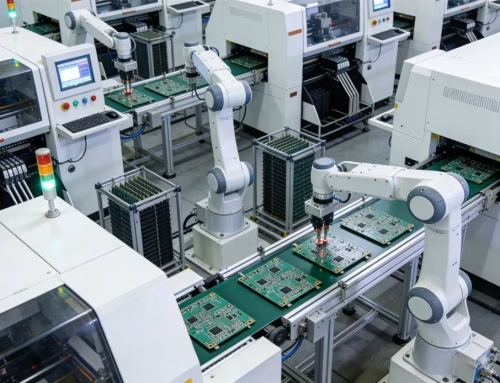
PCB Probe Technology: Ensuring Flawless Electronics

Table of Content
- 1. Na Gaisgich Neo-fhaicsinneach de Chàileachd PCB
- 2. Prìomh Dhleastanas Teicneòlas Sgrùdaidh PCB
- 3. A’ dàibheadh domhainn a-steach do theicneòlasan sgrùdaidh cudromach
- 4. Dùbhlain agus Nuadh-eòlasan ann an Teicneòlas Proba
- 5. Buaidh Sgrùdaidh Adhartach air Càileachd PCBA
- 6. Teicneòlas Pròbhaidh PCBneòlas CÀBHAs
- 7. Geàrr-chunntas
- Na prìomh ghiùlan-bidhe
1. The Unseen Heroes of PCB Quality
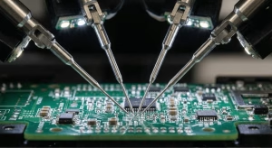
In the intricate world of modern electronics, Printed Circuit Boards(PCBs) are the unsung foundations upon which all digital marvels are built. From the smallest wearable device to the most complex supercomputer, the reliability and performance of a PCB are paramount. As electronic devices continue their relentless march towards miniaturization and higher performance, the density of components on these circuit boards increases dramatically, leaving less and less physical space for traditional testing methods. This evolution has elevated the importance of sophisticated PCB probe technology, transforming it from a mere quality control step into a critical enabler of innovation and reliability.
Ensuring the functionality and integrity of every circuit path and component on a PCB is a monumental task. This is where various types of PCB probes become indispensable. They provide the vital electrical access needed to perform in-circuit testing(ICT), debug issues, conduct quality control checks, and even analyze failures, ultimately guaranteeing that the final electronic product performs as intended. Without precise and efficient probe technology, manufacturers would face overwhelming challenges in detecting defects, leading to costly product recalls and diminished brand reputation. This article will delve into the fascinating world of probe technology, exploring its diverse applications, the innovations driving its advancement, and its crucial role in the modern PCB process.
2. The Critical Role of PCB Probe Technology
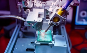
At its core, PCB probe technology is about establishing temporary electrical contact with specific points on a circuit board to measure electrical characteristics or control signals. These “test points” are crucial for verifying the board’s integrity and functionality. In the fast-paced electronics manufacturing environment, accuracy and reliability in probing are non-negotiable. Probes are essential for a wide array of tasks throughout the PCB assembly(PCBA) process, ensuring that the assembled board meets stringent quality standards.
Probes are utilized for everything from circuit testing and debugging to quality control and failure analysis. The specific type of probe employed is highly dependent on the application, reflecting the diverse needs of PCB manufacturers. The fundamental purpose remains consistent: to provide a reliable interface between the complex circuitry of a PCB and the electronic test equipment, allowing for the detection of faults like open circuits, shorts, incorrect component values, or other anomalies that could compromise the board’s performance.
The increasing complexity and density of modern PCBs, especially in compact devices like mobile phones, have led to situations where traditional, dedicated test pads are often abandoned due to space constraints. This trend underscores the need for more innovative and adaptable probe technologies that can maintain comprehensive test coverage without demanding excessive board real estate.
3. Diving Deep into Key Probe Technologies
The landscape of PCB testing is diverse, featuring several distinct probe technologies, each tailored to specific manufacturing stages and requirements. Understanding these different approaches is key to appreciating the depth of modern PCB quality assurance.
3.1 In-Circuit Test(ICT) Probes
In-Circuit Test(ICT) is one of the most established and widely used methods for PCB testing. ICT probes are typically part of a “bed of nails fixture”, a custom-built device that precisely aligns and contacts hundreds or even thousands of spring-loaded probes with specific test points on a PCB. These probes make direct contact with components and traces, allowing the ICT machine to measure voltage, current, resistance , capacitance, and other electrical parameters for each individual component and circuit path on the board. OrinewPCB highlights that ICT probes are excellent for detecting a broad range of faults, including opens, shorts, wrong component values, and polarity issues.
| Feature | Description | Benefit |
| Contact Method | Spring-loaded probes on a fixture | Highly reliable, precise contact |
| Fault Detection | Opens, shorts, component values, polarity | Comprehensive fault coverage |
| Speed | Very fast for volume production | High throughput in manufacturing |
| Cost | High initial fixture cost | Cost-effective for high-volume batches |
While ICT offers comprehensive and fast testing for high-volume production, its main drawback is the significant upfront cost and time associated with designing and manufacturing the custom bed of nails fixture for each unique PCB design. This makes it less ideal for prototyping or low-volume production runs.
3.2 Flying Probe Testing(FPT): The Flexible Alternative
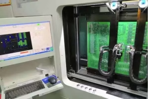
To address the limitations of ICT, particularly for prototypes, low-volume production, or boards with restricted test access, Flying Probe Testing(FPT) emerged as a flexible and fixtureless solution. OrinewPCB explains that FPT utilizes robotic, movable test probes that “fly” across the board to make contact with specific test points. Instead of a fixed array, FPT systems typically employ 2 to 6 independent probes that can move rapidly to any point on the PCB.
The primary advantage of FPT is its flexibility. Since no custom fixture is required, setup times are significantly reduced, and costs are lower for new designs or small batches. This makes FPT an excellent choice for prototype validation, pre-production runs, and even failure analysis. OrinewPCB notes its growing popularity in ensuring circuit boards are manufactured correctly, especially with the evolution of automation and compatibility requirements. However, FPT is generally slower than ICT for mass production due to the sequential nature of its probing.
3.3 Bead Probe Technology(BPT): Addressing Miniaturization
As PCBs become increasingly compact, finding space for traditional test pads for ICT or even accessible points for FPT becomes a significant challenge. This is where Bead Probe Technology(BPT) offers an ingenious solution. OrinewPCB defines BPT as a technique providing electrical ” nodal access” to PCB circuitry for in-circuit testing, specifically making use of small beads of solder placed onto the board’s traces.
These “solder beads” or “solder bumps” are manufactured using the same techniques as other solder features and are placed atop PCB traces, effectively creating miniature test points where standard test pads are not feasible. BPT was first introduced in the 1990s and was originally known as the “Waygood bump”. It is particularly useful when less than 30 mils of space is available for test probe points on the PCB, directly addressing the demands of extreme miniaturization.
However, BPT is not without its challenges. OrinewPCB points out that residual magnetic flux from PCB wiring can sometimes cause poor contact between the probe and the solder bead test point. To counter this, many probe manufacturers have developed specialized, new-type probes specifically designed for bead probe technology, aiming to improve contact performance. The accuracy of the solder-paste printing process is also crucial for consistent bead formation and reliable test access.
4. Challenges and Innovations in Probe Technology
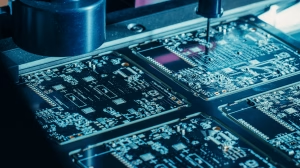
The relentless drive for smaller, faster, and more complex electronic devices presents ongoing challenges for PCB probe technology, demanding continuous innovation.
- Miniaturization and Density:The most significant challenge is the ever-decreasing size of components and the increasing density of circuit board layouts. This leaves minimal space for traditional test points, pushing the limits of probe design and necessitating solutions like BPT.
- Contact Reliability:Ensuring consistent and reliable electrical contact, especially with extremely small test points or solder beads, is critical. Issues like residual magnetic flux can lead to intermittent contact failures, making accurate PCB testing difficult. Innovations in probe tip materials, geometries, and spring forces are continually being developed to enhance contact integrity.
- High Frequencies and Signal Integrity:Modern PCBs often operate at very high frequencies, making signal integrity during testing a concern. Probes must be designed to minimize signal degradation and interference to ensure accurate measurements.
- Cost and Speed Optimization:Manufacturers constantly seek to balance comprehensive test coverage with throughput and cost-effectiveness. The choice between ICT, FPT, and BPT often comes down to this balance, driven by production volume and board complexity. Innovations aim to make FPT faster and more capable for medium-volume production, while ICT systems are becoming more efficient in fixture development.
Manufacturers are also improving the accuracy of processes like solder-paste printing, which is vital for the consistent formation of solder beads in BPT, thereby enhancing test reliability. The development of specialized probes for BPT demonstrates the industry’s commitment to overcoming these challenges and ensuring that advanced PCB designs can still be thoroughly tested.
5. The Impact of Advanced Probing on PCBA Quality
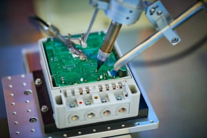
The evolution of PCB probe technology has a profound impact on the overall quality and reliability of electronic products. By providing precise and efficient methods for PCB testing, these technologies contribute to:
- Enhanced Functional Reliability:Thorough testing at the PCB level ensures that individual components and circuit paths are working correctly before final assembly, significantly reducing the chances of product failure in the field.
- Reduced Manufacturing Costs:Catching defects early in the PCBA process , thanks to effective probing, is far less expensive than detecting them during final product testing or, worse, after deployment. This minimizes rework, scrap, and warranty claims.
- Faster Time-to-Market:Efficient testing processes, especially those like FPT that expedite prototype validation, allow manufacturers to bring new products to market more quickly and confidently.
- Improved Design Validation:Probe technologies enable engineers to thoroughly validate new PCB designs, identifying and rectifying potential issues early in the development cycle.
- Consistent Quality Control:Automated probing systems ensure a consistent and repeatable testing process, leading to higher and more predictable product quality across all production batches.
In essence, advanced probe technology acts as a cornerstone of quality assurance in electronics manufacturing, enabling the continued miniaturization, complexity, and reliability demanded by today’s interconnected world. It is a testament to the industry’s commitment to ensuring every electronic device operates flawlessly.
6. PCB Probe Technology FAQs
Question1: What is the primary purpose of PCB probe technology?
The primary purpose is to provide electrical access to specific points on a Printed Circuit Board(PCB) to perform tests, measure electrical characteristics, and identify defects, thereby ensuring the quality and functionality of the board.
Question2: When is flying probe testing(FPT) typically preferred over in-circuit testing(ICT)?
FPT is preferred for prototypes, low-volume production runs, and complex boards with limited space for traditional test pads. Its fixtureless nature offers quick setup and lower initial costs compared to ICT, which requires expensive custom “bed of nails” fixtures.
Question3: What problem does bead probe technology(BPT) aim to solve?
BPT aims to solve the problem of limited space for traditional test pads on highly miniaturized and dense PCBs. By using small “solder beads” on traces as test points, it provides essential nodal access for in-circuit testing where other methods are not feasible due to space constraints.
Question4: How does residual magnetic flux affect probe contact in BPT?
Residual magnetic flux in PCB wiring can interfere with the physical contact between the test probe and the solder bead, leading to poor or inconsistent electrical connections. This necessitates specialized probe designs and accurate solder-paste printing to ensure reliable contact.
7. Summary
Probe technology is an indispensable element in the modern PCB manufacturing and assembly process, ensuring the quality, reliability, and functionality of electronic devices. As electronics continue to miniaturize and become more complex, the demand for sophisticated PCB testing methods grows. Technologies like In-Circuit Test(ICT) offer comprehensive, high-speed verification for mass production, utilizing custom “bed of nails” fixtures. For prototypes and low-volume runs, Flying Probe Testing(FPT) provides a flexible, fixtureless alternative, rapidly “flying” probes across the board to gather data. Addressing extreme miniaturization, Bead Probe Technology(BPT) ingeniously uses small solder beads on traces to create essential “nodal access” points for testing, overcoming the challenge of limited space for dedicated test pads. Despite challenges such as maintaining contact reliability and managing high-frequency signals , continuous innovation in probe design and manufacturing processes is driving these technologies forward, playing a critical role in delivering flawless, high-performance electronics to the market.
Key Takeaways
- PCB probe technology is crucial for verifying the integrity and functionality of circuit boards in an era of miniaturization.
- In-Circuit Testing(ICT) is ideal for high-volume production, offering comprehensive fault detection through custom fixtures.
- Flying Probe Testing(FPT) provides a flexible, cost-effective, and fixtureless solution perfect for prototypes and low-volume PCB testing.
- Bead Probe Technology(BPT) offers vital “nodal access” using solder beads on traces, addressing space constraints on highly dense PCBs.
- Continuous innovation in probe materials and designs is essential to overcome challenges like contact reliability and signal integrity in advanced PCB manufacturing.
OrinewPCB has focused as a one-stop PCB assembly manufacturer from PCB Manufacturing to Electronic Components Sourcing to PCB Assembly to Test to Program IC for more than 14 Years with reliable quality and fastest delivery for global clients.