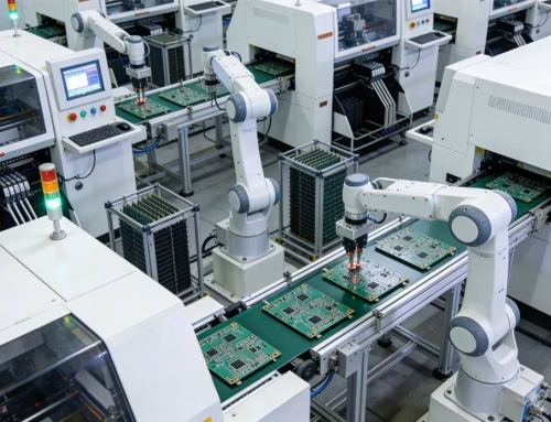
Mastering Miniaturized PCBA Manufacturing

Table of Content
- 1. The Era of Miniaturization
- 2. The Imperative for PCBA Miniaturization
- 3. Key Technologies Driving Miniaturized PCBA Manufacturing
- 4. Advanced Components for Compact Designs
- 5. Precision Assembly Techniques for Miniaturized PCBAs
- 6. Challenges in Miniaturized PCBA Manufacturing
- 7. The Benefits of Miniaturized Electronics
- 8. Future Outlook and Innovations of Miniaturized PCBA
- 9. PCBA Miniaturization FAQs
- 10. Summary
- Key Takeaways
1. The Era of Miniaturization
In an increasingly connected world, the demand for smaller, lighter, and more powerful electronic devices continues to surge. From smart wearables and medical implants to advanced IoT sensors and high-performance computing, the underlying technology enabling this revolution is miniaturized PCBA manufacturing. Printed Circuit Board Assembly(PCBA) miniaturization is no longer a luxury but a fundamental necessity, pushing the boundaries of design, materials science, and manufacturing processes to integrate more functionality into ever-shrinking footprints.
This comprehensive guide delves into the intricate world of PCBA miniaturization, exploring the driving forces behind it, the innovative technologies making it possible, the unique challenges faced, and the profound benefits it delivers. Understanding these aspects is crucial for anyone involved in modern electronics development and production.
2. The Imperative for PCBA Miniaturization
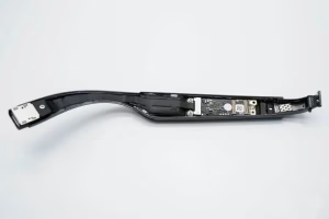
The push for smaller electronics stems from several key market demands and technological advancements:
- Consumer Electronics:Smartphones, smartwatches, and virtual reality headsets constantly strive for sleek designs, longer battery life, and enhanced features, all while maintaining a compact form factor.
- Medical Devices:Implantable devices, diagnostic tools, and portable health monitors require extreme miniaturization for patient comfort, efficacy, and discreet integration.
- Internet of Things(IoT):Billions of connected devices, often deployed in constrained spaces or remote locations, necessitate tiny, energy-efficient PCBAs.
- Aerospace and Defense:Miniaturized electronics are critical for drones, satellite systems, and advanced weaponry where space and weight are at a premium, without compromising performance or reliability.
- Automotive Industry:Advanced driver-assistance systems(ADAS), in-car infotainment, and electric vehicle control units benefit from compact, high-performance electronics.
Achieving this level of compactness requires a concerted effort across the entire electronics design and manufacturing ecosystem, focusing on innovative PCB assembly techniques and cutting-edge components.
3. Key Technologies Driving Miniaturized PCBA Manufacturing
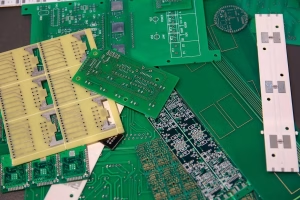
The foundation of PCBA miniaturization lies in advancements in PCB design and fabrication. High Density Interconnect(HDI) PCBs are at the forefront of this evolution, allowing for significantly higher component density and routing complexity.
High Density Interconnect (HDI) PCBs
HDI PCB technology is paramount for miniaturized designs. These boards utilize a combination of smaller traces, microvias, and stacked vias to create much denser circuitry than conventional PCBs. Key features include:
- Microvias:These are tiny holes(typically <150µm in diameter) that connect different layers of a PCB. Unlike traditional through-hole vias, microvias conserve valuable board space and reduce signal path lengths.
- Buried and Blind Vias:Buried vias connect internal layers without penetrating the outer layers, while blind vias connect an outer layer to one or more inner layers without going all the way through the board. Both types free up space on external layers for component placement.
- Finer Lines and Spaces:HDI boards can feature conductor lines and spaces as small as 25µm(1 mil), enabling more complex routing within a smaller area.
- Stacked Vias:This advanced technique allows microvias to be stacked directly on top of each other, further increasing routing density and enabling more complex layer interconnections.
The ability of HDI PCB technology to pack more functionality into a smaller area makes it indispensable for modern PCBA miniaturization projects.
4. Advanced Components for Compact Designs
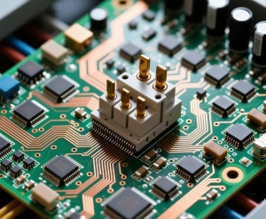
The physical size of electronic components is a major factor in PCBA miniaturization. Manufacturers are continually developing smaller packages without compromising performance or reliability.
- Miniature SurfaceMount Devices(SMDs): The industry has moved from larger 0805 and 0603 packages to incredibly tiny 0402, 0201, 01005, and even 008004 packages for resistors and capacitors. These microscopic components require extreme precision during PCB assembly.
- System-in-Package(SiP) and Multi-Chip Modules(MCMs):SiP technology integrates multiple integrated circuits(ICs) along with passive components into a single package, often with advanced packaging techniques like flip-chip or wire bonding. This reduces board space dramatically and improves performance by minimizing inter-chip distances.
- Embedded Components:Embedding passive components(resistors, capacitors) directly into the PCB layers further saves surface area and shortens electrical paths, improving signal integrity and reducing electromagnetic interference(EMI).
- Wafer-Level Chip-Scale Packages(WLCSPs):These are essentially ICs packaged directly on the wafer, offering the smallest possible package size and direct connection to the PCB.
Selecting the right miniature components is a critical aspect of successful miniaturized PCBA manufacturing.
5. Precision Assembly Techniques for Miniaturized PCBAs
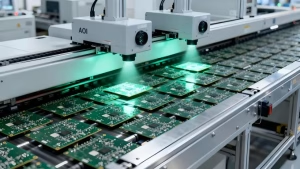
As components shrink and board designs become denser, the PCB assembly process demands unparalleled precision and control.
- Advanced Solder Paste Printing:Fine-pitch components require highly accurate solder paste deposition. Stencils with smaller apertures and advanced printing techniques(e.g., jet printing) are essential to ensure consistent and precise solder volume.
- High-Precision Pick-and-Place Machines:Modern pick-and-place equipment must handle microscopic components(like 01005s and smaller) with extreme accuracy, often employing vision systems for precise alignment. The placement accuracy can be as fine as a few microns.
- Reflow Soldering Optimization:Customized reflow profiles are crucial to prevent issues like tombstoning, voiding, or bridging with miniature components. Temperature ramps, soak times, and peak temperatures must be meticulously controlled.
- Flux Chemistry:Specialized no-clean fluxes are often preferred for miniaturized assemblies to reduce post-assembly cleaning challenges and potential damage to delicate components.
- Underfill and Conformal Coating:For enhanced reliability, especially in rugged or medical applications, underfill materials are used beneath fine-pitch BGAs and CSPs to reinforce solder joints, while conformal coatings protect the entire assembly from environmental factors .
Each step in the PCB assembly process for miniaturized boards requires a high degree of automation and expertise to maintain quality and yield.
6. Challenges in Miniaturized PCBA Manufacturing
While the benefits are clear, PCBA miniaturization introduces significant challenges throughout the product lifecycle:
| Challenge Area | Description | Impact on Miniaturization |
| Design Complexity | Routing dense circuits with fine lines and microvias, managing impedance, and ensuring signal integrity. | Requires sophisticated CAD tools, DFM/DFL considerations, and expert designers. |
| Thermal Management | Concentrating more power in a smaller area generates higher heat density, which can degrade component performance and reliability. | Demands innovative cooling solutions, thermal vias, and careful component placement. |
| Manufacturing Precision | Handling and placing microscopic components, achieving consistent solder joints, and avoiding defects. | Necessitates high-tolerance equipment, cleanroom environments, and stringent process control. |
| Testability | Reduced space for test points, making in-circuit testing(ICT) difficult or impossible. | Leads to reliance on boundary scan, functional testing, and X-ray inspection. |
| Rework and Repair | Repairing defects on boards with ultra-fine pitch components and buried/blind vias is extremely challenging and often impractical. | Emphasizes “first-time-right” manufacturing and robust process controls. |
| Material Selection | Finding substrate materials that offer excellent electrical performance, thermal stability, and mechanical strength in thin formats. | Requires advanced dielectric materials, often with higher cost. |
| Supply Chain | Sourcing miniature, high-performance components can be complex due to lead times, availability, and cost. | Demands strong supplier relationships and proactive inventory management. |
7. The Benefits of Miniaturized Electronics
Despite the challenges, the advantages offered by miniaturized PCBA manufacturing are compelling and drive continuous innovation:
- Reduced Form Factor and Weight:The most obvious benefit, enabling sleeker products and enhancing portability. Crucial for wearables, drones, and medical implants.
- Increased Functionality:More features can be packed into the same or smaller volume, enhancing device capabilities without increasing overall size.
- Improved Performance:Shorter signal paths on compact boards reduce propagation delays, minimize electromagnetic interference(EMI), and improve signal integrity, leading to faster and more reliable operation.
- Lower Power Consumption:Often, smaller components and shorter traces contribute to reduced power usage, extending battery life in portable devices.
- Enhanced Durability:Smaller, lighter boards are often less susceptible to physical stress and vibration, leading to greater mechanical reliability.
- Cost Efficiency(Indirectly):While initial manufacturing costs can be higher, miniaturization can lead to cost savings in overall product design, packaging, and logistics. It also enables new product categories and market opportunities.
8. Future Outlook and Innovations of Miniaturized PCBA
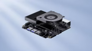
The trajectory of PCBA miniaturization points towards even greater integration and sophistication. Emerging trends include:
- Ultra-fine Pitch Technology:Continued development of even smaller component packages(e.g., 008004 and beyond) and associated assembly capabilities.
- Advanced Packaging:Further advancements in 3D packaging, heterogeneous integration, and chiplets to create highly integrated modules.
- AI and Automation:Artificial intelligence and machine learning will play an increasing role in optimizing design for manufacturability(DFM), simulating thermal and electrical performance, and enhancing automated PCB assembly processes.
- Novel Materials:Research into new substrate materials with superior electrical, thermal, and mechanical properties will enable even thinner and more reliable boards.
- Additive Manufacturing:3D printing of PCBs and electronic structures offers unprecedented freedom in design and integration, potentially revolutionizing how complex, miniaturized devices are created.
The journey of miniaturized PC BA Manufacturing is one of continuous innovation, pushing the boundaries of what is possible in electronics.
9. PCBA Miniaturization FAQs
Question1: What is the smallest component size currently used in PCBA miniaturization?
While 01005(0.4 x 0.2 mm) is common for high-density applications, some specialized designs are now incorporating 008004(0.2 5 x 0.125 mm) passive components.
Question2: What is the primary driver for PCBA miniaturization?
The main driver is the increasing consumer and industrial demand for smaller, lighter, and more portable electronic devices across various sectors like wearables, medical implants, IoT sensors, and smart automotive systems, all while maintaining high performance and functionality.
Question3: How does an HDI PCB contribute to miniaturization?
An HDI PCB enables miniaturization by using fine lines and spaces, microvias, and buried/blind vias to route more circuitry in a smaller area, allowing for higher component density and more compact designs.
Question4: What are the biggest challenges in soldering miniature components?
The primary challenges include achieving precise solder paste deposition, ensuring accurate component placement, preventing bridging between closely spaced pads, and managing thermal profiles to avoid defects like tombstoning.
Question5: Can existing PCB assembly lines be easily adapted for miniaturized manufacturing?
While some existing lines can be upgraded, significant investments in high-precision pick-and-place machines, advanced solder paste printers, and sophisticated inspection equipment are often necessary to handle the extreme tolerances required for miniaturized PCBA manufacturing.
10. Summary
Miniaturized PCBA manufacturing is an essential discipline for the modern electronics industry, driven by an insatiable demand for smaller, more functional, and efficient devices. This field leverages cutting-edge technologies like HDI PCB design, advanced components suchaging, and ultra-precise PCB assembly techniques to condense complex circuitry into incredibly small footprints. While these advancements bring forth significant challenges in design, thermal management, manufacturing precision, and testing, the benefits of reduced size and weight, increased functionality, and improved performance are profound. As technology continues to evolve, the future promises even more integrated and intelligent miniaturized solutions, further transforming every aspect of our connected world.For projects requiring compact, high-density electronics, reliable PCB manufacturing and assembly capabilities are essential for turning miniaturized designs into production-ready products.
Key Takeaways
- PCBA miniaturization is critical for developing modern devices across consumer, medical, IoT, and industrial sectors.
- HDI PCB technology, with its microvias and fine line routing, forms the backbone of compact circuit designs.
- The use of ever-smaller components(e.g., 01005, SiP) and advanced packaging is crucial for achieving high density.
- PCB assembly for miniaturized boards requires extreme precision in solder paste application, component placement, and ref low soldering.
- Key challenges include complex design, thermal management, difficult testing, and demanding rework processes.
- Benefits include smaller form factor, increased functionality, improved performance, and enhanced durability.
- Future trends point towards further integration, AI-driven manufacturing, and novel material applications.