HDI PCB
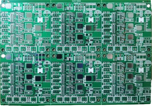
Table of Content
- Define the HDI construction before requesting a price
- Review fabrication and component assembly as one release
- Every bare PCB receives flying-probe electrical testing
- From bare boards to genuine-component turnkey PCBA
- Nine PCBA quality stages with an agreed test scope
- Plan delivery from the complete release package
- Request a HDI PCB review
- HDI PCB questions
ORINEWPCB · FABRICATION TO TURNKEY ASSEMBLY
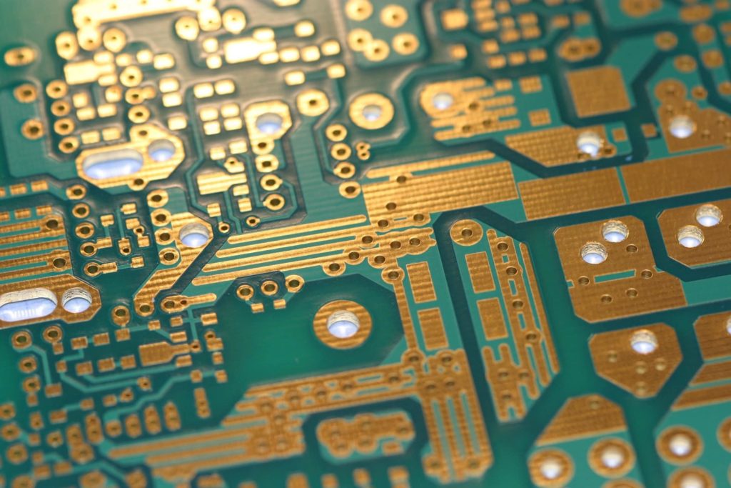
HDI PCB manufacturing is appropriate when routing density or package escape requires fine features and microvia-based interconnections. The buying decision starts with an agreed stack-up and via structure, not just the term “HDI.” Send the design for a fabrication review before locking the build cost or schedule.
Define the HDI construction before requesting a price
Blind vias connect an outer layer to an internal layer; buried vias connect internal layers without reaching an outer surface. Microvias support dense interconnection, but via depth, registration, filling and the lamination sequence must match the actual construction. A smaller board is not automatically an easier or cheaper build.
On a small screen, swipe the table horizontally. Keyboard users can focus the table region and use the arrow keys.
| Decision | Send or confirm | Why it matters |
|---|---|---|
| Stack-up and build-up | Layer order, dielectric thicknesses, copper and the intended build-up structure. | Sequential lamination and material decisions affect manufacturability and scheduling. |
| Via structure | Microvia start/stop layers, stacked or staggered arrangement and through-hole details. | An unambiguous drill table helps prevent a different structure being quoted. |
| Via-in-pad requirements | Identify pads requiring via filling, capping or planarization and the acceptance scope. | The fabrication interface must support the intended soldering process. |
| Fine-pitch assembly | Package MPNs, pitch, placement orientation and hidden-joint locations. | Review paste printing, handling and agreed inspection coverage alongside board fabrication. |
| Electrical performance | Controlled-impedance nets, target values, tolerances and required evidence. | A general electrical test is not an impedance measurement or an RF performance test. |
Review fabrication and component assembly as one release
Dense packages often make board fabrication and assembly interdependent. Before purchasing, check whether the routing escape, via-in-pad treatment, pad definition and component land pattern describe the same design intent. If a change is proposed, review its electrical and assembly effects before approving it.
- Supply Gerber/drill files and a fabrication drawing with a clear via layer map.
- Confirm the proposed stack-up before final impedance-sensitive routing is released.
- Identify critical packages and provide the manufacturer land-pattern requirements.
- Agree hidden-joint inspection and any programming or functional test procedure.
- Freeze approved changes and keep the BOM, placement data and board files synchronized.
Every bare PCB receives flying-probe electrical testing
OrinewPCB flying-probe tests every bare PCB we manufacture, not just a sample. This checks the conductive networks against the electrical test data. Include your netlist where available and identify any required test parameters or records in the RFQ.
An electrical pass does not establish every physical characteristic, controlled impedance, RF performance, thermal reliability or finished-product function. Specify those requirements and any additional evidence separately. This keeps the acceptance scope clear before fabrication begins.
From bare boards to genuine-component turnkey PCBA
Keep the fabrication, BOM purchasing and assembly review connected when you need a finished assembly. Small-to-medium batches and high-mix turnkey PCB assembly are a particular OrinewPCB strength. List quantities and differences for each design or variant so the release is unambiguous.
We supply and use 100% brand-new, original, genuine electronic components for customers’ turnkey assemblies. Our cooperation with manufacturers and distributors helps us seek competitive BOM pricing and practical lead times. Exact MPNs, current availability, permitted sources and delivery dates are checked for your project; alternatives require customer approval.
Bare PCB supply
Release the fabrication data, quantity, acceptance scope and delivery needs.
BOM sourcing
Send full manufacturer part numbers, quantities, approved alternatives and documentation needs.
One-stop assembly
Combine fabrication, sourcing, assembly and the agreed inspection or test plan.
Explore one-stop PCB assembly, electronic component sourcing and the OrinewPCB brand website.
Nine PCBA quality stages with an agreed test scope
When the order includes assembly, our quality workflow covers nine stages. The applicable inspection plan and evidence are agreed for the actual build:
- IQC: incoming materials.
- SPI: solder paste inspection.
- Online AOI: in-line optical inspection.
- SMI: first-article inspection.
- IPQC: in-process quality checks.
- Offline AOI: post-solder optical inspection.
- X-ray: hidden joints to the agreed scope.
- Manual QC: workmanship review.
- Pre-shipment QA: identification, quantity and packaging.
These are nine quality stages, not nine functional tests. Programming, ICT, functional testing or application-specific validation need an agreed procedure, access or fixtures, and pass/fail criteria. See our factory and quality workflow.
Plan delivery from the complete release package
We work toward the earliest practical delivery for the approved scope. Send the required quantity, design variants and target date, and state whether it means production completion, dispatch or arrival. Materials, engineering questions, assembly preparation and agreed tests all affect the confirmed schedule.
Compare quotations using the same material, revision, sourcing responsibility and acceptance scope. A lower bare-board or placement line item is not automatically a lower complete project cost.
Related planning: Controlled impedance requirements · Prototype PCB manufacturing · One-stop PCB assembly.
Request a HDI PCB review
Send OrinewPCB your files and tell us what you need: bare boards, BOM sourcing or a complete turnkey assembly. Files are optional for an initial discussion.
- Board files, drawing revision and special material or construction requirements
- Quantity per design or variant and repeat-order expectations
- BOM with full MPNs, placement and assembly drawings if assembly is needed
- Inspection, programming, functional-test and documentation requirements
- Target date, delivery destination and any staged shipment needs
For direct email: [email protected]. A quote request does not authorize purchasing, substitutions or production.
HDI PCB questions
Does every multilayer PCB need HDI construction?
No. Use the routing, package escape and product constraints to determine whether HDI is needed. A conventional multilayer structure may be suitable when the design can meet its requirements without build-up microvias.
Are stacked and staggered microvias interchangeable?
Do not treat them as interchangeable. Their geometry and manufacturing requirements differ. State the intended structure and approve any proposed change through the fabrication review.
Will flying-probe testing prove HDI long-term reliability?
No. Electrical testing checks the conductive networks under the agreed test conditions. It does not replace material, construction, process qualification or any reliability testing required by the product.
Related Posts

ORINEWPCB · PROJECT SUPPORT
Contact Us
Discuss your PCB assembly project with our team.
FREE QUOTE
Plan your turnkey PCBA build.
Share your quantity and requirements. Add Gerber files and a BOM when ready.
Files are optional for an initial discussion. Include any assembly, sourcing or testing requirements in your message.