PCB Probe Testing: Flying Probe, ICT & Test-Point Checklist

Table of Content
ORINEWPCB · PCBA TEST PLANNING
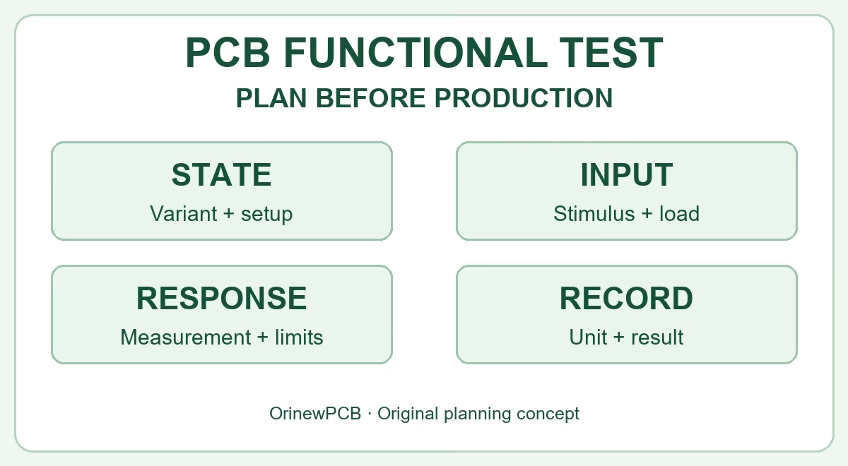
Which PCB probe test should you choose? Start with the faults you need to detect, available test access and expected production volume. Flying probe testing often suits changing designs and smaller batches because it avoids a dedicated bed-of-nails fixture. Fixture-based in-circuit testing (ICT) can suit stable, repeat production. Neither method automatically verifies every product function: agree the test coverage and any powered functional test separately.
For turnkey PCB assembly, define the test plan before the board layout and quotation are final. A request for “PCB testing” alone leaves too much room for different interpretations.
What PCB probe testing does—and what a pass means
PCB probe technology provides temporary electrical contact with accessible pads, leads or other approved targets. The tester uses those contacts to make programmed measurements. A passing result means that the board met the limits in that particular test program; it is not a promise of flawless operation in every environment.
First distinguish the item being tested. Bare-board electrical testing checks a fabricated PCB against its connectivity requirements before components are assembled. Assembled-board testing examines the populated PCBA, where components and parallel circuit paths affect the measurements. A supplier’s bare-PCB flying probe result does not establish that the assembled product has passed functional testing.
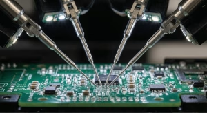
Flying probe vs fixture-based ICT vs functional test
These approaches answer different questions. In this guide, “ICT” refers to the fixture-based approach for comparison; moving-probe systems can also perform in-circuit measurements. Confirm the actual tester configuration and proposed coverage instead of relying only on the method name.
On a phone, swipe the table sideways. You can also focus the table region and use the arrow keys.
| Decision | Flying probe | Fixture-based ICT | Functional test |
|---|---|---|---|
| Physical access | Moving probes contact programmed targets. | A dedicated fixture contacts many defined nodes. | Product connectors or a project-specific interface. |
| Typical planning fit | Prototypes, design changes and smaller batches. | Stable designs with repeat production. | Boards needing verification of specified operating functions. |
| Preparation | Program, access review and board handling. | Fixture, program, support and maintenance planning. | Procedure, firmware, power, loads and pass/fail limits. |
| Main trade-off | Probe movement can increase cycle time. | Upfront tooling and revision-change costs. | Coverage depends on the implemented scenarios. |
| Ask in the RFQ | Which nets and components can be checked? | What does the fixture and program include? | Which functions, conditions and results will be recorded? |
Flying probe: flexible access, with real limits
Flying probe testing uses independently moving probes rather than a board-specific bed-of-nails fixture. Probe count, one-sided or double-sided access, supported measurements and available powered-test functions depend on the machine and its configuration. Do not specify a universal number of probes or assume that every system performs the same tests.
Ask for an access and coverage review of the actual board revision. Tall components, inaccessible connections and board handling can affect the feasible program. “Fixtureless” does not mean no engineering, no setup or zero nonrecurring cost.
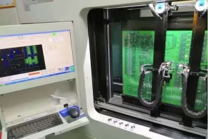
ICT and functional testing: agree complementary coverage
Fixture-based ICT is useful for production screening and fault isolation, but inaccessible nodes and circuit interactions can leave gaps. Functional testing checks agreed behavior with the required power, firmware and interfaces. A board that passes structural checks may still need functional verification.
Related brand guides: in-circuit testing and flying probe testing. Available scope, tooling and acceptance requirements must be confirmed for your project.
PCB test-point checklist before layout release
Do not copy a generic pad diameter or pitch into every design. Request the intended tester or fixture supplier’s design rules, then confirm them against the board stack, component heights and electrical requirements. Use this checklist in the design-for-test review:
- List the measurements first. Identify the faults and critical circuits to be checked, the required nodes, and any accepted coverage gaps.
- Map each required node to physical access. Record its net name, coordinates, board side and target type. Check that the target remains accessible after assembly.
- Confirm target geometry. Agree pad size, spacing, solder-mask opening and suitable contact surface with the test engineer. A via is not automatically a suitable probe target.
- Check the approach path. Review tall connectors, shields, heatsinks and nearby components. Include board edges, panel features, clamps and any underside support.
- Review mechanical loading. Agree board support and permissible probing force so the test interface does not create unacceptable flexing or damage.
- Protect sensitive circuits. Discuss high-speed, high-impedance and sensitive analog nodes before adding targets; test access must not compromise the design.
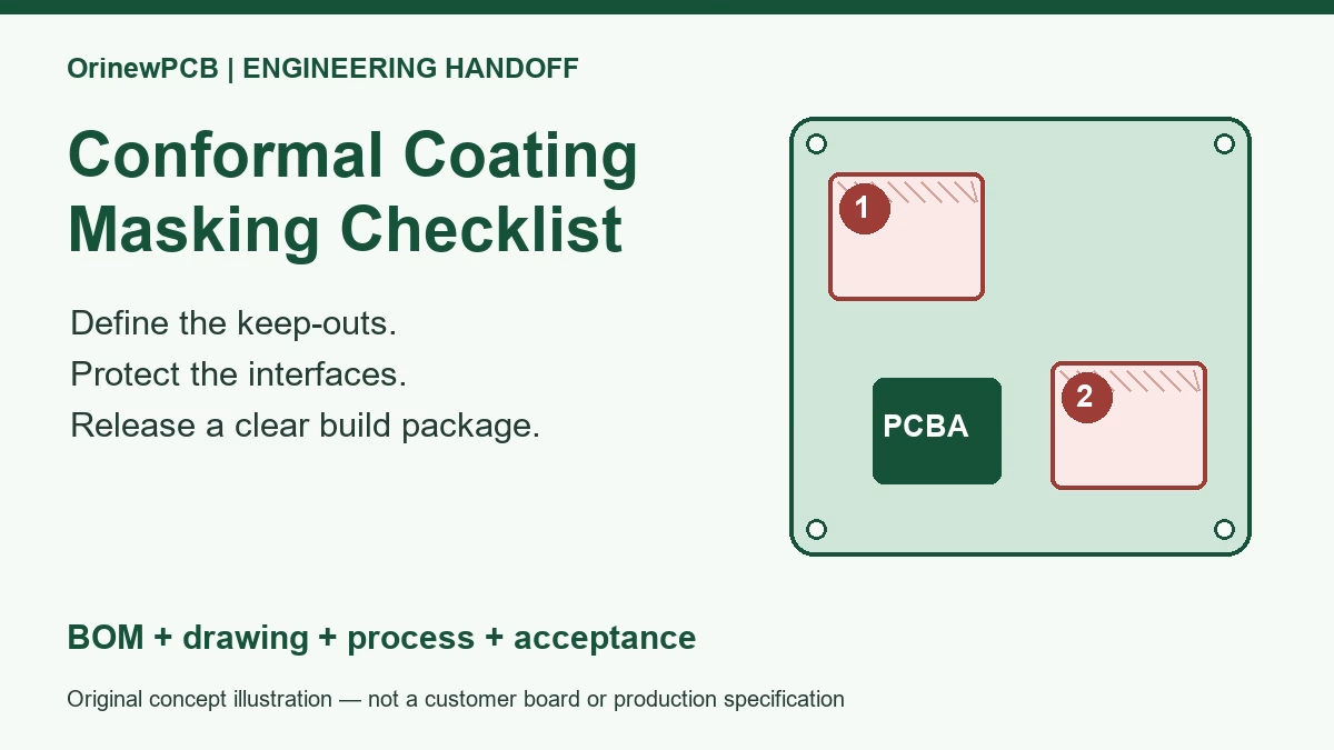
- Plan access after later operations. Decide whether testing occurs before coating, shielding or enclosure assembly. Document any required masking and subsequent checks.
- Release consistent data. Match the schematic, layout, netlist, BOM, placement data and assembly drawing to the same revision and build variant.
Use the PCB assembly drawing guide to communicate orientation, DNP variants and special operations alongside the test requirements.
Contact problems and bead probe technology
A test failure needs diagnosis. Poor contact can produce a false call, while a genuine component or assembly fault requires corrective action. Soldering flux residue left on a contact target can interfere with reliable electrical contact. Include the surface condition in the investigation.
Bead probe technology creates small, intentional solder features on suitable traces to provide electrical access where ordinary pads are difficult to accommodate. It requires coordinated layout, solder-mask, stencil and test-interface design. Probe force and contact with the bead are part of the implementation; this is not a general instruction to add solder bumps to arbitrary traces.
When investigating intermittent contact, record the affected target, repeatability and visible condition. Review contamination, probe wear, alignment, support and the approved contact method with the test engineer. Avoid repeatedly pressing or scraping the board to force a pass. Preserve the initial failure information and document the disposition.
Compare total test cost—not a universal quantity threshold
There is no single batch size at which every project should switch from flying probe to ICT. Ask for comparable quotations covering the same board revision, intended coverage and reporting. Include tooling, programming, test cycle, maintenance, revision changes and retest policy.
Planning example, not an OrinewPCB price: for an early pilot with a likely layout change, ask about program changes and requalification. For a stable repeat build, ask whether fixture investment changes the cost per accepted board. In either case, compare what is tested before comparing the total.
Comparison worksheet: total quoted test cost = agreed one-time development/tooling + quantity × quoted per-board test charge + any separately quoted maintenance or revision work.
Do not treat a lower test charge as an equivalent offer if it excludes powered checks, report retention or important inaccessible nets. Ask each supplier to state the exclusions and assumptions.
What to send for a turnkey PCBA test quotation
For a combined turnkey PCB assembly quotation, connect the test scope with PCB fabrication, component sourcing and assembly from the start. The table below is a practical RFQ worksheet, not a mandatory file-format standard.
| Input | Include | Decision it supports |
|---|---|---|
| Board identity | Part number, revision, variant and provisional-file flags. | Prevents quoting or testing the wrong build. |
| Manufacturing data | Agreed PCB data, BOM, placement file and assembly drawing. | Connects fabrication and assembly scope. |
| Test access data | Schematic, available netlist/layout export and test-point map. | Supports access and coverage review. |
| Production plan | Pilot quantity, expected repeat batches and likely design changes. | Supports tooling and program decisions. |
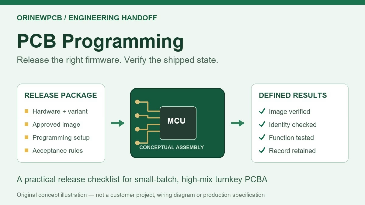
| Functional requirements | Firmware revision, programming method, procedure, loads, limits and expected results. | Defines the powered-test work. |
| Acceptance and records | Required checks, excluded coverage, traceability, report format and failure handling. | Defines release evidence and responsibilities. |
If you only need bare PCB manufacturing or electronic component sourcing, state that scope clearly. For a full assembly, tell us which materials you will supply and which OrinewPCB should source. Components alone do not define the finished board’s test coverage.
PCB probe testing FAQ
Is flying probe testing the same as functional testing?
No. Flying probe describes a moving-probe access approach. Functional testing verifies specified operating behavior. Some systems support selected powered functions, but the agreed program determines what is actually checked.
Does a bare-PCB electrical test cover the assembled board?
No. It checks the unpopulated PCB. Component installation, programming and product functions need their own agreed inspection and test plan after assembly.
Can flying probe test every BGA solder joint?
Do not assume so. Hidden connections and electrical access constrain coverage. Ask for a review of the actual package, nets and available complementary methods rather than a blanket BGA-coverage promise.
What test-point size should I use?
Obtain the proposed test system’s rules before layout release. Agree target dimensions, spacing, side access, height clearances and contact surface for that design. A generic minimum is not a substitute for the review.
Is bead probe technology another name for flying probe?
No. A bead is an intentionally designed solder contact feature. Flying probe describes moving test probes. Confirm compatibility of the contact feature and selected test interface.
Does “100% tested” mean every possible defect is detected?
No. It may mean every board was run through a particular program. Ask which measurements, functions and limits are included, what is inaccessible and what records show the result.
Can I request a quote before the test procedure is final?
Yes. Share the available files and mark open decisions. Ask for a preliminary scope with explicit assumptions. Confirm the final procedure, limits, tooling and responsibilities before production release.
What should I include in an OrinewPCB inquiry?
Send your board revision, available PCB files, BOM, placement data, quantities and intended tests. Include programming, reporting, target date and destination requirements. Files can follow after the initial discussion.
Request PCB assembly with a defined test scope
Make the test plan part of your turnkey PCBA quotation. Send OrinewPCB the files you have and the questions still open. Ask us to review PCB fabrication, BOM sourcing, assembly and the proposed test scope together.
Copy this inquiry outline: “Please quote turnkey PCBA for [board/revision/variant], [pilot quantity] and [planned repeat quantity]. We need [structural/powered functional/programming checks]. Test files and limits are [attached/pending]. Please identify access gaps, tooling/program charges, exclusions and required inputs. Target date and destination: [details].”
Prefer an initial discussion? Contact our team or email [email protected]. Final scope, price and schedule follow project review.
Related Posts
ORINEWPCB · PROJECT SUPPORT
Contact Us
Discuss your PCB assembly project with our team.
FREE QUOTE
Plan your turnkey PCBA build.
Share your quantity and requirements. Add Gerber files and a BOM when ready.
Files are optional for an initial discussion. Include any assembly, sourcing or testing requirements in your message.