Industrial Control PCBA: The Core Driving Force of Modern Industry

Industrial control PCBA is the physical foundation that determines the performance limits and lifespan of industrial equipment. It must complete signal closed-loop control within nanosecond timing to ensure micron-level motion precision, while simultaneously withstanding temperature cycles from -40°C to 125°C, 20G vibration, and intense electromagnetic interference. This dual pursuit of precision and reliability fundamentally distinguishes its technical system from consumer electronics. This article analyzes the key technical core of industrial control PCBA across four dimensions: design, materials, process, and testing.
1 Definition of Industrial Control PCBA
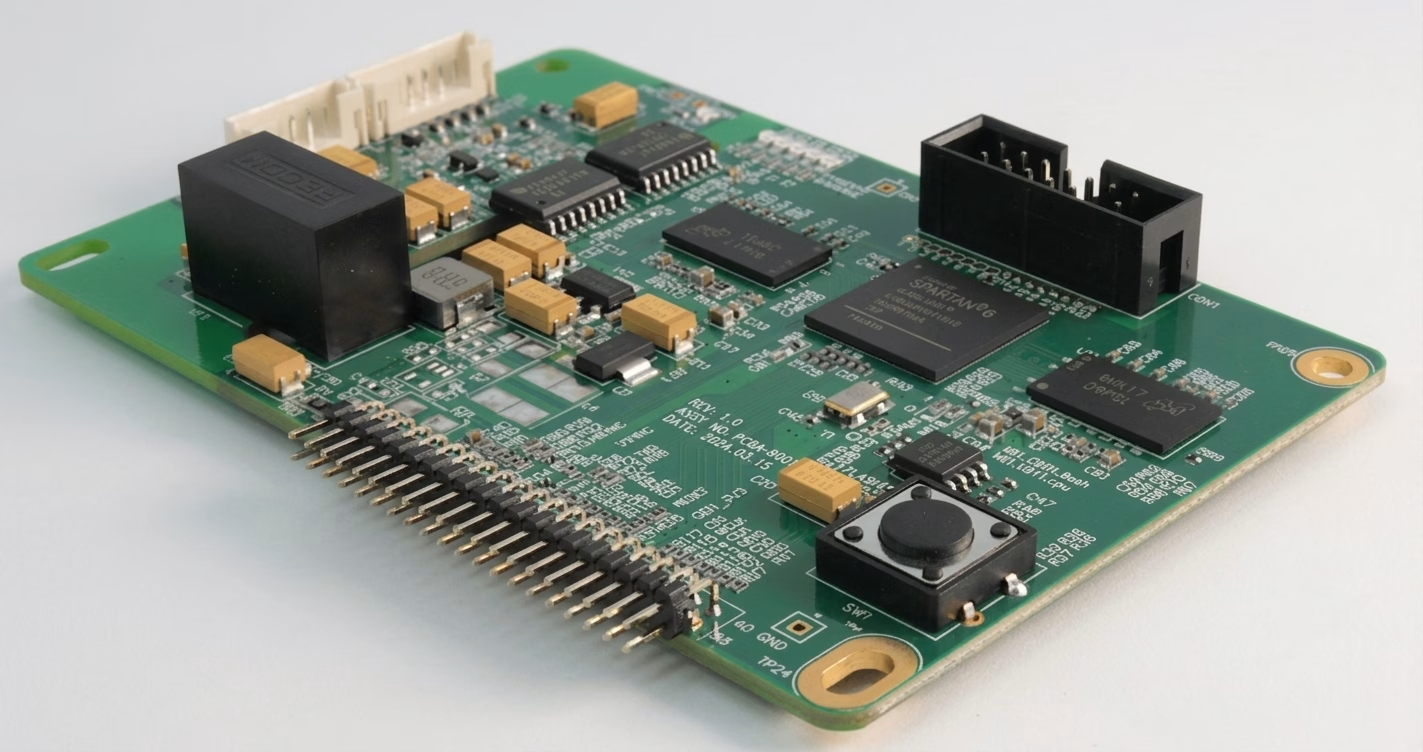
1.1 Technical Boundaries of Industrial Control PCBA
Industrial control PCBA (Printed Circuit Board Assembly) refers to printed circuit board assemblies designed for industrial automation, process control, motion control, and related applications. Its design objective is to ensure 10-15 years of continuous and stable operation under harsh conditions including wide temperature ranges, strong electromagnetic interference, persistent vibration, and high humidity.
From the perspective of technical parameters, industrial control PCBA must satisfy the following boundary conditions:
- Operating Temperature Range: -40°C to +85°C (standard industrial grade), extendable to -55°C to +125°C (military/automotive grade)
- Vibration Resistance: Compliant with IEC 60068-2-6 standard, withstands 5-500Hz random vibration with peak acceleration up to 20G
- Insulation Resistance: ≥100MΩ @500V DC
- Dielectric Withstand Voltage: AC 1500V/60s without breakdown
- Mean Time Between Failures (MTBF): ≥100,000 hours
1.2 Layer Structure and Material System
Industrial control PCBA typically adopts a 4-32 layer multilayer board structure with clearly defined layer functions:
| Layer Type | Functional Positioning | Typical Design Parameters |
| Signal Layer | High-speed/low-speed signal transmission | Impedance control ±10%, differential pair intra-pair skew ≤5mil |
| Power Layer | Multi-voltage domain power supply | Copper thickness ≥2oz, partitioned isolation design |
| Ground Layer | Signal return path and shielding | Complete copper plane, split gap ≤1/20 wavelength |
| Shielding Layer | EMI suppression | Distance to ground layer ≤0.2mm |
The base material system primarily uses high-Tg FR-4, with Tg value ≥170°C and Z-axis coefficient of thermal expansion (CTE) ≤60ppm/°C, ensuring no delamination occurs during multiple reflow cycles and long-term high-temperature operation.
1.3 Parameter Comparison with Consumer-Grade PCBA
| Technical Parameter | Consumer-Grade PCBA | Industrial-Grade PCBA | Difference Factor |
| Design Life | 3-5 years | 10-15 years | 3× |
| Operating Temperature | 0°C to 40°C | -40°C to 85°C | Temperature range expanded 4× |
| Copper Foil Thickness | 1oz (35μm) | 2-10oz (70-350μm) | Up to 10× |
| Minimum Trace Width/Spacing | 4/4 mil | 3/3 mil (down to 2.5/2.5) | Precision improved 25% |
| Defect Rate Requirement | ≤500ppm | ≤100ppm | 5× stricter |
| Test Coverage | Sampling (approx. 60%) | Full inspection (≥95%) | Coverage increased 35% |
2 Key Technologies in Industrial Control PCBA Design
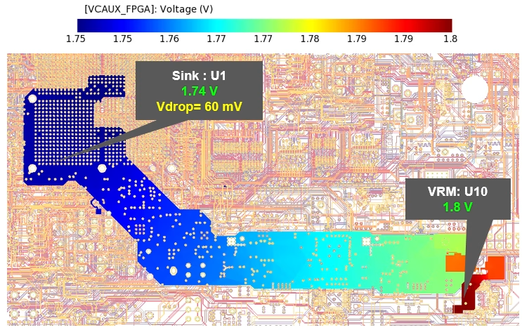
2.1 Power Integrity (PI) Design
In industrial control equipment, high-power motor drives, IGBT switching power supplies, and similar modules generate significant power fluctuations. The core objective of power integrity design is to maintain supply voltage ripple ≤±5%.
Specific design methods include:
- Multi-layer Stacking Strategy: Adopt a stack-up structure of four or more layers such as “Signal-Ground-Power-Signal”, enabling the power and ground planes to form a planar capacitance effect. This enhances high-frequency decoupling capability by more than 40%.
- Decoupling Capacitor Network: Configure by frequency segmentation—100nF (high frequency, >100MHz), 1μF (mid frequency, 10-100MHz), 10μF (low frequency, ≤10MHz)—to form a broadband decoupling network.
- Partitioned Power Supply: Physically separate analog and digital circuit power planes, connecting them at a single point via ferrite beads or 0Ω resistors to isolate digital noise from interfering with analog signals.
Empirical data shows that industrial control boards with optimized PI design reduce bit error rates by 82% compared to standard designs during grid voltage fluctuations.
2.2 Signal Integrity (SI) Design
Encoder feedback in servo drives and gigabit data transmission in industrial Ethernet impose stringent requirements on signal quality. The core metrics of SI design involve controlling signal reflection, crosstalk, and timing skew.
Key technical parameters and implementation methods:
| Design Consideration | Parameter Requirement | Implementation Method |
| Impedance Matching | ±10% (±5% for high-speed signals) | Calculate trace width/dielectric thickness using Polar Si9000; differential impedance 100Ω±10% |
| Length Matching | Intra-pair ≤5mil, inter-group ≤50mil | Serpentine routing compensation; use 45° or arc corners |
| 3W Rule | Trace spacing ≥3× trace width | Parallel routing length ≤500mil; insert ground isolation traces for longer runs |
| Crosstalk Suppression | ≤-30dB @1GHz | Guard traces for critical signals; place GND vias on both sides of sensitive traces |
For encoder signals in servo drives, SI optimization can control signal distortion within 0.1ns, ensuring positioning accuracy at the micron level.
2.3 Thermal Management Design
Thermal failure of high-power components is the primary failure mode in industrial control PCBA. When junction temperature exceeds the rated value by 10°C, device lifespan is halved.
Engineering methods for thermal design:
- Thermal Via Array: Arrange thermal vias with 0.3-0.5mm diameter and 1.0mm pitch around power component pads, reducing thermal resistance by approximately 30%.
- Copper Foil Thickness Selection: Use 2-3oz copper foil for high-current paths. The relationship between current-carrying capacity and temperature rise follows the IPC-2152 standard—1oz copper, 1mm trace width carries approximately 1A (with 10°C temperature rise).
- Embedded Heat Dissipation: Embed copper coins within the multilayer board to directly contact the bottom of power chips, reducing junction temperature by 22°C at 100W load.
- Thermal Simulation Verification: Analyze temperature field distribution using CFD (Computational Fluid Dynamics) software to ensure hotspot temperature ≤105°C.
One PLC manufacturer reduced power device junction temperature by 35°C and increased MTBF to 100,000 hours by designing an embedded copper-based heatsink beneath critical chips.
2.4 Electromagnetic Compatibility (EMC) Design
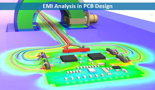
Industrial environments contain strong sources of electromagnetic interference such as variable frequency drives, welding machines, and high-power relays. Industrial control PCBA must pass EN 55032 Class A radiated emission testing.
Core strategies for EMC design:
- Layer Stack Shielding: Place critical signal layers between two complete ground layers, creating a Faraday cage effect that enhances radiation suppression by over 15dB.
- Interface Filtering: Deploy π-type filters (capacitor-ferrite bead-capacitor) at each I/O port. Select cutoff frequency based on signal speed—50MHz for low-speed I/O, 500MHz for high-speed communication.
- Protection Components: Parallel TVS diodes at power entry (response time ≤1ns); series ferrite beads on signal lines (impedance ≥600Ω at 100MHz).
- Zoned Layout: Partition circuits by noise level into “clean zone” (analog/digital core), “transition zone” (interface circuits), and “dirty zone” (power/relay circuits), with spacing ≥3mm.
2.5 Design for Manufacturability (DFM)
DFM serves as the bridge connecting design and volume production. DFM specifications for industrial PCBA are over 30% stricter than those for consumer-grade products.
Key DFM parameters:
- Trace Width/Spacing: Outer layers ≥4mil, inner layers ≥3mil (safe values for mass production).
- Pad Design: BGA pad diameter per IPC-7351 standard, deviation ≤±0.05mm; 0402 resistor pad dimensions 0.8×0.4mm.
- Process Edge: Reserve width ≥5mm; tooling hole diameter ≥1.0mm.
- Panel Utilization: Use matrix panelization to achieve material utilization ≥90%.
- Teardrop Pads: Add teardrops at all pad-to-trace connections to enhance peel strength.
A rail transit equipment manufacturer reduced wave soldering defect rate from 3% to 0.5% and increased single-board first-pass yield to 99.2% by optimizing DFM specifications.
3 Material Selection and Validation System
3.1 Substrate Material Selection Criteria
The glass transition temperature (Tg) of the substrate is the primary indicator distinguishing industrial-grade from consumer-grade laminates. Tg value determines the mechanical stability of the board at elevated temperatures.
| Laminate Grade | Tg Value | Z-axis CTE | Typical Application |
| Standard FR-4 | 130-140°C | 70-80 ppm/°C | Consumer electronics |
| Mid-Tg FR-4 | 150-160°C | 55-65 ppm/°C | General industrial control |
| High-Tg FR-4 | 170-180°C | 45-55 ppm/°C | Industrial control/automotive electronics |
| Ultra-High Tg | ≥200°C | ≤40 ppm/°C | Military/aerospace |
Selection principle: Industrial control products require minimum Tg≥150°C, with Tg≥170°C recommended. High-frequency applications require specialty materials such as Rogers RO4350B (Dk=3.48±0.05, Df=0.0037@10GHz) or Panasonic MEGTRON6 (Df=0.002@10GHz).
3.2 Copper Foil Specifications and Current-Carrying Design
Industrial control PCBA often carry high currents. Copper foil thickness selection directly determines temperature rise and reliability.
| Copper Thickness | Ounce (oz) | Thickness (μm) | Current Capacity of 1mm Trace Width (10°C Rise) |
| 0.5oz | 0.5 | 17.5 | 0.5A |
| 1oz | 1.0 | 35 | 1.0A |
| 2oz | 2.0 | 70 | 1.8A |
| 3oz | 3.0 | 105 | 2.5A |
| 10oz | 10.0 | 350 | 6.0A |
For motor drives, power modules, and similar applications, outer layer copper ≥2oz and inner layer ≥1oz is common practice. Heavy copper boards (≥3oz) require stepped etching processes to compensate for undercut effects.
3.3 Surface Finish Process Comparison
Surface finish affects pad solderability, planarity, and corrosion resistance.
| Finish Type | Thickness | Planarity | Solderability | Corrosion Resistance | Typical Application |
| HASL (Hot Air Solder Leveling) | 1-40μm | Poor | Good | Fair | Consumer grade |
| ENIG (Electroless Nickel Immersion Gold) | Au 0.05-0.1μm/Ni 3-5μm | Excellent | Excellent | Excellent | BGA/fine-pitch components |
| Immersion Silver | 0.1-0.4μm | Excellent | Excellent | Prone to oxidation | High-frequency/high-speed |
| Hard Gold | Au≥3μm/Ni 5-8μm | Excellent | Excellent | Superior | Edge connectors/frequent insertion |
| OSP (Organic Solderability Preservative) | 0.2-0.5μm | Excellent | Good | Fair | Lead-free soldering |
Industrial control PCBA preferentially uses ENIG finish—the nickel layer provides a diffusion barrier, while the gold layer protects the nickel from oxidation, enabling multiple reflow cycles and high solder joint reliability.
3.4 Component Selection and Derating Design
Components represent the weak link in PCBA reliability. Industrial control products must follow strict derating design guidelines:
| Component Type | Derating Requirement | Selection Standard |
| Resistor | Power derating ≥50% | Operating voltage ≤70% of rated voltage |
| Capacitor | Voltage derating ≥50% (electrolytic ≥80%) | Temperature rating ≥105°C |
| IC | Junction temperature derating ≥20°C | Industrial grade (-40°C to 85°C) or automotive grade (-40°C to 125°C) |
| Connector | Current derating ≥50% | Gold plating thickness ≥15μ” |
| Crystal Oscillator | Industrial grade (-40°C to 85°C) | Frequency stability ≤±50ppm |
All active components must pass AEC-Q100 (automotive grade) or equivalent industrial-grade qualification. Memory chips and processors must support wide-temperature operation.
4 Precision Manufacturing Process Control
4.1 Lamination Process Parameter Control
The lamination quality of multilayer boards determines Z-axis reliability. Delamination is a typical failure mode for industrial control PCBA during temperature cycling.
Key process parameters:
- Lamination Pressure: ≥400psi, ensuring resin flows sufficiently to fill circuit gaps.
- Heating Ramp Rate: 2-3°C/min to prevent bubble formation.
- Dwell Time: Maintain at Tg temperature for ≥60min to complete resin crosslinking and curing.
- Dielectric Layer Thickness Uniformity: Deviation <10%.
- Vacuum Level: ≤50mbar to eliminate interlayer bubbles.
After lamination, boards must pass three cycles of 288°C/10s solder float testing without delamination or blistering.
4.2 Drilling and Hole Metallization
Vias represent the most stress-concentrated structures in PCBs. Barrel cracks and copper fractures are primary failure modes under vibration.
Process control considerations:
- Drilling Accuracy: CNC drilling positional accuracy ±25μm; deburr after drilling.
- Hole Size Specifications: Mechanical holes ≥0.2mm; blind/buried vias (laser drilled) ≥0.1mm.
- Hole Wall Copper Thickness: Average ≥20μm; minimum point ≥18μm.
- Copper Elongation: ≥10% to ensure resistance to thermal stress.
- Desmear: Plasma cleaning to remove resin residue from hole walls, improving electroless copper adhesion.
HDI board blind vias use CO2 laser drilling at 35-45mJ energy. Bottom copper thickness must be ≥15μm to ensure interconnection reliability.
4.3 Trace Formation and Etch Compensation
Trace width accuracy directly affects impedance control. Undercut effects during etching cause actual trace width to be less than designed.
Precision control measures:
- Imaging Technology: Use LDI (Laser Direct Imaging) to achieve minimum trace width/spacing of 3/3mil
- Etch Compensation: Preset compensation based on copper thickness—1oz compensates 0.5mil, 2oz compensates 1.0mil, 3oz compensates 1.5mil.
- AOI Inspection: 100% inspection of each layer with detection accuracy of 0.02mm.
- Impedance Verification: Perform TDR testing on first article; control 100Ω differential impedance within ±5%.
4.4 SMT Assembly Process Window
The width of the SMT process window determines volume production yield. Industrial control boards often have narrower process windows due to diverse component types and mixed packaging.
Core control parameters:
- Solder Paste Selection: Type 3 powder (particle size 25-45μm); SAC305 alloy (Sn96.5/Ag3.0/Cu0.5).
- Printing Accuracy: Stencil thickness 0.1-0.15mm; printing speed 25-50mm/s; separation speed 1-3mm/s.
- Placement Accuracy: Chip components ±0.05mm; BGA/CSP ±0.03mm.
- Reflow Profile: Ramp rate 1-3°C/s; time above liquidus 60-90s; peak temperature 235-245°C.
- Temperature Differential Control: ΔT between BGA and surrounding small components ≤5°C.
One industrial control module manufacturer reduced BGA voiding rate from 12% to 2.8% and increased production yield from 85% to 99.2% by optimizing pad design (deviation ≤0.05mm) and reflow profile.
4.5 Conformal Coating and Protection Process
Conformal coating serves as the final line of defense for industrial control PCBA against harsh environments. Coating process selection must match the application scenario.
| Coating Material | Temperature Range | Dielectric Strength | Key Characteristics | Typical Application |
| Acrylic (AR) | -40 to 125°C | 40kV/mm | Good moisture resistance, repairable | General industrial environments |
| Polyurethane (UR) | -40 to 130°C | 35kV/mm | Chemical corrosion resistance | Chemical/pharmaceutical |
| Silicone (SR) | -40 to 200°C | 20kV/mm | Good flexibility, wide temperature range | High vibration/extreme temperatures |
| Epoxy | -40 to 150°C | 45kV/mm | High hardness, wear resistant | Mechanical protection required |
Coating Thickness Control: Dry film thickness 30-50μm (per IPC-CC-830 standard). Selective coating equipment uses programmable robotic arms for precise spraying, avoiding keep-out areas such as connectors and switches. Thickness uniformity is controlled within ±5μm.
5 Test Verification and Reliability Assessment
5.1 Electrical Performance Testing
Electrical testing serves as the final barrier against functional defects. Industrial control boards require test coverage ≥95%:
| Test Type | Test Content | Acceptance Criteria |
| Flying Probe/ICT | Continuity, resistance, capacitance, inductance | Resistance error ±5% |
| Insulation Resistance | Insulation between adjacent nets | ≥100MΩ @500V DC |
| Dielectric Withstand | Between high-voltage and low-voltage circuits | AC 1500V/60s no breakdown |
| Impedance Testing | Differential/single-ended impedance | Target value ±10% (±5% for high-speed) |
ICT test fixtures can measure up to 1280 test points simultaneously. Flying probe testing is used for small-to-medium batches to verify uncovered nodes.
5.2 Environmental Stress Screening
Environmental testing exposes early-life failures and screens out “infant mortality” defects:
| Test Item | Test Condition | Duration | Failure Criteria |
| Temperature Cycling | -40°C ↔ 125°C, transition time ≤1min | ≥500 cycles | Resistance change ≤10% |
| Damp Heat Aging | 85°C/85%RH, bias voltage applied | 1000 hours | Insulation resistance ≥10MΩ |
| Mechanical Vibration | 5-500Hz, 20G peak | 2 hours per axis | No solder joint cracks |
| Salt Spray Test | 5% NaCl, 35°C | 96 hours | No significant corrosion |
5.3 Microstructural Analysis
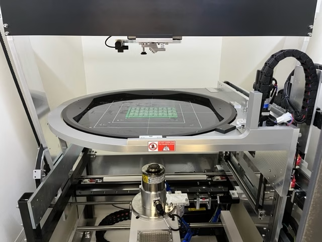
Microstructural analysis evaluates process quality and failure mechanisms:
- X-Ray Inspection: Check BGA voiding rate (required ≤25%) and inner layer registration accuracy (±50μm).
- Metallographic Cross-Section: Measure hole wall copper thickness (≥18μm), IMC layer thickness (1-3μm), and interlayer bonding condition.
- SEM/EDS: Analyze solder joint microstructure, element migration, and intermetallic compound composition.
- Infrared Thermography: Map temperature distribution under operating conditions to identify hotspots (temperature rise gradient ≤15°C/min).
5.4 Long-Term Reliability Verification
Given the long-life requirements of industrial control products, accelerated life testing is necessary to assess long-term reliability:
- Highly Accelerated Life Test (HALT): Gradually increase temperature (-100 to 170°C) and vibration (up to 50Grms) stresses until failure, determining operational and destruct limits.
- High Temperature Operating Life (HTOL): Operate at 125°C and rated voltage for 1000 hours without functional failure.
- CAF (Conductive Anodic Filament) Test: 85°C/85%RH with 100V bias for 1000 hours; insulation resistance ≥10⁸Ω.
- Temperature Humidity Bias (THB): Verify resistance to ion migration.
6 FAQs
(1)Why must industrial control PCBs use high-Tg laminates?
Tg (glass transition temperature) is the critical temperature point at which the laminate transitions from a glassy state to a rubbery state. Above Tg, the Z-axis expansion coefficient of the board increases sharply by 3-5 times, subjecting the hole wall copper to significant tensile stress that can cause cracking and failure. Industrial control equipment often operates in 85°C ambient environments. Combined with component self-heating, localized board temperatures can reach 100-120°C. If standard FR-4 with Tg=130°C is used, the operating temperature approaches the Tg point, inevitably leading to long-term failure. Industrial control boards require minimum Tg≥150°C, with Tg≥170°C recommended, ensuring a safety margin of over 50°C.
(2)What special processes are required for 3oz and thicker heavy copper boards?
Three major challenges exist: ① Undercut Control—Thicker copper results in more severe lateral etching. Preset compensation is required (3oz compensates 1.5mil). ② Lamination Resin Filling—The high aspect ratio of gaps between heavy copper traces makes complete resin filling difficult. High-flow prepreg, increased lamination pressure (≥450psi), and extended dwell time (≥90min) are necessary to prevent voids. ③ Solder Mask Coverage—Large height differences in traces can cause insufficient solder mask thickness at corners. Double printing or curtain coating processes are required to ensure corner thickness ≥10μm.
(3)How is BGA voiding rate controlled?
IPC-7095 requires voiding rate ≤25%. A three-pronged approach is used: Solder Paste and Stencil—Select low-voiding solder paste; use “cross” or rounded-square stencil apertures to facilitate outgassing. Reflow Profile—Extend preheat time (60-90s) to fully volatilize flux; maintain time above liquidus at 60-90s with peak temperature 240-245°C. Pad Design—Follow IPC-7351 standard; pad diameter ≈0.8× ball diameter. With optimization, voiding rate can be reduced to within 5%.
(4)What are the challenges in achieving ±5% impedance control?
While standard ±10% tolerance is relatively lenient, ±5% requires comprehensive tight control: Material Variation—Standard laminates have Dk batch-to-batch variation of ±5%; specialty laminates with Dk tolerance ≤±2% are required. Trace Width Tolerance—A 1mil change in trace width shifts impedance by 2-3Ω. LDI exposure is needed to lock trace width within ±0.5mil. Dielectric Thickness—A 10μm variation in lamination thickness shifts impedance by approximately 1.5Ω; thickness tolerance must be held within 5%. Production Closed-Loop—Perform TDR testing on first article of each batch; adjust trace width compensation if deviation exceeds ±5%.
(5)How to select the appropriate conformal coating?
Select material based on environmental conditions: High humidity/condensation → Acrylic (AR), best moisture resistance; Salt spray/corrosive gases → Polyurethane (UR), strong chemical resistance; High vibration/thermal shock → Silicone (SR), good flexibility without cracking; Repair required → Acrylic (AR), solvent-removable for easy rework. Coating thickness should be controlled per IPC-CC-830 with dry film thickness of 30-50μm.
(6)What is the shelf life of industrial PCBA?
Bare PCB—ENIG finish boards 12 months; OSP finish boards 6 months (beyond this, 125°C baking for 4-8 hours is required for moisture removal). Assembled PCBA—12-24 months in sealed ESD-protective packaging. Boards stored beyond their shelf life must be baked before assembly; otherwise, moisture vaporization during reflow can cause delamination or blistering. Soldering must be completed within 72 hours after baking.
8 Summary
The reliability of industrial control PCBA is a systematic engineering discipline integrating design, materials, process, and testing. The design phase requires embedding reliability at the source through PI/SI simulation and thermal analysis. The materials phase demands strict adherence to high-Tg laminates, heavy copper foil, and industrial-grade component selection. The manufacturing phase necessitates micron-level precision control in lamination, drilling, etching, and assembly. The testing phase relies on multi-dimensional verification encompassing electrical, environmental, microstructural, and long-life assessments. A thorough understanding of this technical chain is essential for equipment manufacturers to evaluate supply chain capability and mitigate risks at the design source. As Industry 4.0 advances toward higher integration (Any-layer HDI), higher frequencies (112Gbps PAM4), and greater intelligence (embedded condition monitoring), only by implementing reliability principles throughout the entire process can the solid hardware foundation for intelligent manufacturing be established.