
The Complete Guide to PCBA Testing

Table of Content
In the life cycle of modern electronic products, printed circuit board assembly (PCBA) serves as the crucial physical foundation from the conception of a single chip to the finished device in the end-user’s hands. The quality and reliability of a PCBA directly determine a product’s performance, lifespan, and market reputation. Consequently, PCBA testing acts as the “gatekeeper” and “quality judge.” This article provides an in-depth yet accessible guide to PCBA testing, covering its definition, types, core technologies, and related design considerations.
1. PCBA Testing Fundamentals – Definition, Scope, and Value
1.1 What is a PCBA?
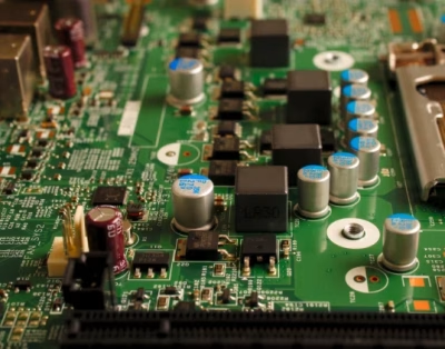
PCBA stands for Printed Circuit Board Assembly. It refers to the process of soldering various electronic components (resistors, capacitors, integrated circuits, connectors, etc.) onto a bare PCB that already has conductive traces, forming a complete circuit module or product motherboard. Essentially, the PCBA is the beating heart of an electronic device.
1.2 Definition and Core Objectives of PCBA Testing
PCBA testing encompasses a series of verification procedures performed after components are soldered onto the PCB. These tests validate electrical performance, functionality, reliability, and manufacturing quality. The core objectives are:
- Ensure Correct Electrical Connections:Detect basic defects like shorts, opens, and cold solder joints.
- Verify Component Functionality:Confirm all components meet design specifications and were not damaged during soldering.
- Guarantee Overall Functional Implementation:Ensure the entire PCBA operates as intended, with proper software and hardware integration.
Assess Long-Term Reliability: Simulate real-world environmental stresses to verify product lifespan and stability.
- Control Process Quality:Identify manufacturing defects at various stages early, preventing them from moving downstream and reducing costs.
1.3 The Three-Layer Testing Structure
PCBA testing is a systematic process, typically divided into three layers throughout the production flow:
- Component Inspection:Testing incoming electronic components (sampling or 100%) before placement to ensure their quality. This is the “first line of defense.”
- Bare PCB Test: Testing the blank PCB before component assembly, primarily checking for opens, shorts, and other manufacturing defects in the traces. Common methods include flying probe test or dedicated fixture testing.
- PCBA Test:This is the focus of this guide—comprehensive testing of the fully assembled module, ranging from simple connectivity checks to complex functional and reliability validation.
2. Design for Test – PCB Design Considerations for Testability
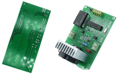
- Test Points:
Necessity: These are the most critical element of Design for Test (DFT). Test points are metal pads or vias on the PCB reserved for contact by test probes.
Design Principles: Test points should provide access to key nets and component pins. They must be placed away from tall components for easy probe access, have sufficient size and spacing, and be designed with signal integrity in mind for critical signals (e.g., clocks, high-speed signals), sometimes requiring series resistors for isolation.
- Test Traces:
Dedicated “test traces” with test points can be added for analog signals or critical sensitive lines. This allows engineers to connect oscilloscopes or logic analyzers to observe signal quality under actual operating conditions, greatly aiding debug and fault diagnosis.
- Diagnostic Aid Design:
LED Indicators: Placing LEDs at power inputs, near power pins of key chips, or beside functional modules provides immediate visual feedback. A simple on/off state quickly indicates power presence, chip activation, or module functionality, aiding rapid fault isolation.
Test Headers and Jumpers: Including standard interfaces or selective connection jumpers facilitates isolating circuit blocks, injecting test signals, or reading internal states, enhancing test flexibility and depth.
3.Panoramic View of PCBA Test Technologies
Various PCBA test methods exist, categorized by stage, target, and purpose. They are often combined in production to form a multi-tiered test strategy.
3.1 Electrical Performance Testing: Verifying the Circuit’s “Lifeblood”
These tests check basic electrical connections and parameters.
- In-Circuit Test (ICT):
Principle: Uses a custom “bed-of-nails” fixture with hundreds/thousands of probes contacting test points on the PCBA underside. It rapidly measures component values (resistance, capacitance, inductance) and checks for opens/shorts in networks, with or without power applied.
Pros: Very fast, high fault coverage (often >90%), ideal for high-volume production, and can pinpoint faults to specific components/nets.
Cons: High fixture cost and long lead time; fixtures are typically product-specific, offering low flexibility.

- Flying Probe Test:
Principle: Uses a small number (typically 4-8) of precision, program-controlled probes that move across the PCBA surface, contacting test points sequentially for measurement.
Pros: No expensive fixture needed, highly flexible setup, short development time. Ideal for low-volume production, prototypes, and quick-turn samples.
Cons: Test speed is slower due to probe movement.
ICT and Flying Probe tests are often complementary: Flying Probe for low-volume verification and test program debug before fixture fabrication, and ICT for high-volume production of mature products.

3.2 Visual and Internal Inspection: The Machine’s “Keen Eye”
These tests use optical or radiographic methods to inspect physical structure and solder quality without electrical signals.
- Automated Optical Inspection (AOI):
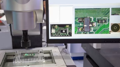
Principle: Uses high-resolution cameras to capture images of the PCBA from multiple angles. It automatically identifies visual defects by comparing images to a known-good “golden board” or pre-defined algorithmic rules. Defects include missing/wrong components, incorrect polarity, misalignment, tombstoning, solder bridges, and bent leads.
Pros: Non-contact, fast, detects many visual defects, and can be integrated into the line for real-time monitoring.
Cons: Cannot inspect solder joints under components like BGAs or QFNs. Susceptible to false calls due to reflectivity or color variations.
- X-Ray Inspection (AXI):
Principle:Using the ability of X-rays to penetrate materials, perform transillumination imaging of PCBA. Different materials (solder, copper, silicon) absorb X-rays differently, creating image contrast. This allows clear inspection of hidden solder joints (e.g., BGA balls), internal traces, and plated through-hole integrity.
Pros: The ultimate method for inspecting BGA voids, bridges, insufficient solder, and internal defects in multilayer boards.
Cons: Very expensive equipment, relatively slow inspection speed. Often used for sampling or 100% inspection of high-reliability products.
AOI and X-Ray together form a complete visual inspection system from 2D external appearance to 3D internal structure.

3.3 Functional Test (FCT): Simulating the Real “Stage Performance”
This is the test closest to the product’s actual use case.
- Principle:The PCBA is placed in a simulated or real operating environment (often connecting to peripheral loads, sensors, displays, etc.). It is powered on, and predefined input signals (e.g., button presses, communication commands, simulated sensor inputs) are applied. The output responses (e.g., voltage, current, waveforms, data packets, screen display, motor rotation) are then checked to verify if all designed functions are fully realized.
- Characteristics:
“Black Box” Testing: The tester focuses on input/output conformity to specifications, not internal circuit details.
Highly Customized: FCT fixtures and software must be developed specifically for the product, potentially involving complex test logic and protocols (e.g., USB, Bluetooth, Wi-Fi testing).
Final Validation: This is often the last and most comprehensive performance gate before PCBA shipment.

3.4 Reliability Testing: The “Stress Test” Pushing Limits
Reliability tests are not necessarily performed on every PCBA but are key to evaluating whether the product design, materials, and process can withstand time and environmental challenges.
- Burn-in / Aging Test:
Purpose: Subjects PCBAs to extended operation under high temperature and possibly elevated load (or overvoltage) conditions. This accelerates internal electrochemical reactions and forces out latent defects (e.g., early component failures, solder joint fatigue), screening out “infant mortality” failures. It ensures products shipped to customers are in the stable “random failure” period of their lifespan.
- Environmental Stress Testing:
Temperature Cycling: Simulates thermal expansion/contraction from day/night cycles or device power cycling, testing the resistance of solder joints, PCB materials, and components to thermal fatigue.
Humidity / Damp Heat Testing: Evaluates the PCBA’s insulation performance and corrosion resistance in humid environments.
Vibration and Drop Testing: Simulates mechanical stress during shipping, installation, and use, testing solder joint strength and structural integrity.
4.Building an Efficient PCBA Test Strategy and Process
No single test method catches 100% of defects. Therefore, a hierarchical, combined test strategy is essential.
A typical test flow for a high-reliability product PCBA might be:
- Incoming Material Inspection(Components)
- Bare Board Test(PCB)
- Solder Paste Inspection (SPI)after printing
- Pre-Reflow AOIafter component placement
- Post-Reflow AOI
- Selective X-Ray Inspection(for BGAs/key components)
- In-Circuit Test (ICT)
- Functional Test (FCT)
- Burn-in/Aging Test(sampling or 100%)
- Final Visual Inspection & Packing
The strategy differs based on production volume and phase:
- Prototype / Low-Volume Phase:A “Flying Probe Test + Functional Test” combination is recommended for its high flexibility and low initial investment.
- High-Volume Mature Product Phase:An “ICT + AOI + Functional Test” combination is typical, prioritizing high coverage and efficiency. X-Ray and Reliability tests are added based on product requirements.
5. FAQs
Flying Probe Test: Best suited for low-volume production, prototyping, and R&D phases. No expensive custom fixtures are needed, offering great flexibility. However, its test speed is relatively slow.
ICT (In-Circuit Test): Ideal for high-volume manufacturing of stable designs. Requires a custom “bed-of-nails” fixture, involving a higher initial investment. The key advantage is extremely fast test speed, making it cost-effective for mass production.
AOI (Automated Optical Inspection): Uses cameras to inspect the board surface. Primarily detects visual defects like wrong/missing components, misalignment, solder bridges, etc. It’s fast and has a lower operational cost.
X-Ray Inspection: Uses X-rays to see inside the assembly. Primarily inspects hidden solder joints (e.g., under BGAs, QFNs) for voids, bridges, and can also detect internal PCB layer issues. The equipment is much more expensive and the inspection process is slower.
Follow a structured approach: “From outside in, from system to component.”
Check Power Supplies: Verify all voltage rails and ripple/noise are within spec.
Check Critical Signals: Use an oscilloscope to probe key clocks, reset, and enable signals.
Check Communication: Verify data on primary communication buses (e.g., UART, I2C, SPI).
Isolate Modules: Disconnect or simulate peripheral modules to narrow down the faulty section.
Best Practice: Apply scientifically justified stress levels (e.g., 10-20°C above max operating temp) and durations (typically 48-168 hours) based on the product’s application. This screens out weak units while avoiding excessive wear on good ones.
Use a Tiered Strategy: Employ fast methods like AOI/ICT to catch the majority of defects, reserving more complex and time-consuming FCT for final deep validation.
Prioritize: Mandate 100% coverage for safety-critical and core functions (e.g., power circuits). Requirements can be relaxed for secondary features.
Adapt Dynamically: Focus on high coverage during new product introduction (NPI). Once production stabilizes, optimize the strategy for cycle time and cost.
Beyond just adding test points, designers often forget:
Test Point Accessibility: Ensure probe clearance around tall components.
Separate Power Rail Access: Provide individual test points for each voltage rail.
Protect High-Speed Signals: Place a small series resistor before the test point on sensitive traces to minimize probe loading effects.
Include Debug Aids: Add features like status LEDs or test headers (e.g., UART) for quick functional checks.
Opt for Flying Probe Test: One machine handles many different boards, eliminating fixture costs and lead times.
Use a Universal Fixture Platform: Platforms with vacuum plates and adjustable/removable probe arrays allow for quick changeovers.
Modularize Test Programs: Build reusable software modules for common tests (power, communications). New projects can then rapidly assemble a test sequence from these blocks.
Monitor Trends: Track yield in real-time; get alerts on any dips for immediate investigation.
Find Root Causes: Analyze which defect types are most frequent and at which process step, enabling targeted process improvements.
Optimize Strategy: Identify test items that never fail; consider simplifying or removing them to save time.
Support Decisions: Use data to justify decisions like equipment upgrades or component supplier changes.
6. Summary
PCBA testing is the bridge connecting design and manufacturing, ensuring products transition reliably from blueprint to finished goods. It is not an isolated step but a quality assurance system integrated throughout the product realization process. Understanding and effectively applying various test technologies, combined with a scientific test strategy, is key not only to intercepting defects and reducing costs but also to building an excellent brand and earning market trust. For electronic engineers, project managers, and quality professionals, mastering the complete knowledge framework of PCBA testing is an essential capability for successfully navigating complex electronic product development.
If you are in need of PCBA assembly services and unsure where to turn, please consider Orinew Tech Co., Ltd. With 14 years of experience, we provide one-stop PCBA solutions—from component procurement and PCB fabrication to full assembly. Supported by a comprehensive and rigorous inspection process, we deliver only high-standard, premium-quality PCBA products.








