
The Complete Guide to High Frequency PCB Communication Circuits

Today’s data-driven world requires instant transmission of information for technological progress to continue apace. From smartphone communication and self-driving cars, to 5G networks and deep space exploration – one key component plays an integral part: the High-Frequency Printed Circuit Board (HF PCB).
High-Frequency PCBs differ from their counterparts by being designed specifically to carry and process electromagnetic signals between 500 MHz and 100 GHz and beyond. No longer simply simple electrical connectors, their performance determines speed, accuracy and reliability in an entire system. This guide explores core features, materials design challenges applications and future prospects of High-Frequency PCBs showing why they are essential in modern high-tech industries.
1. Introduction to High-Frequency PCBs

High-Frequency PCBs are specially designed circuit boards used for transmitting radio frequency (RF), microwave and millimeter wave signals. When signal frequencies reach hundreds megahertz or higher, their characteristics begin to shift away from being simply wires to strong “wave” properties; at this point common materials like FR-4 (an epoxy glass laminate) fail due to signal loss and unstable electrical behavior.
High-Frequency PCBs aim to facilitate low-loss, low-distortion signal transmission with minimal loss and distortion in challenging physical environments such as aircraft or missile testing facilities. They utilize special substrate materials, precise manufacturing and strict design rules in order to achieve Signal Integrity (SI) and Power Integrity (PI), maintaining clean high-frequency signals as they travel. Therefore, High-Frequency PCBs should not be seen as standard components – they’re vital engineering elements which define performance limits for advanced communications, radar or high speed computing systems.
2. Key Properties of High-Frequency PCBs
High-frequency PCBs stand out with their superior performance due to a set of carefully chosen material properties, which work together as the basis for high frequency applications.
| Characteristic | Description | Role and Importance |
| Low Dielectric Constant (Dk) | Measures a material’s ability to store electrical energy. A lower value indicates a reduced ability to store charge. | Enables faster signal propagation with less delay, which is crucial for systems requiring extreme timing accuracy. |
| Low Dissipation Factor (Df) | Measures the tendency of a material to convert electromagnetic energy into waste heat. A lower value indicates less conversion. | Minimizes signal attenuation (insertion loss), ensuring signal strength over longer distances, reducing the need for boosters and lowering system power consumption. |
| Stable Temperature Coefficient (TCDk) | Measures the stability of the Dielectric Constant (Dk) with changes in temperature. An ideal value is near zero. | Ensures stable circuit performance (e.g., center frequency, filter bandwidth) over a broad temperature range (e.g., -55°C to +125°C), as required in military or automotive applications. |
| Low Coefficient of Thermal Expansion (CTE) | Measures the rate of expansion of a material when heated. | Ensures dimensional compatibility with copper foil, preventing via breakage and circuit damage during soldering or operation, which is critical for long-term reliability. |
| High Thermal Conductivity | Measures a material’s ability to conduct heat. | Effectively transfers heat away from hot spots generated by high-power devices and signal loss, preventing localized overheating that degrades performance and shortens lifespan. |
| Dimensional Stability and Low Water Absorption | Measures a material’s resistance to changes in size during processing and its tendency to absorb moisture. | Dimensional stability ensures the accuracy of precision transmission lines; low water absorption prevents moisture from altering the material’s Dk and Df, thereby avoiding signal distortion. |
3. Key Materials of High-Frequency PCBs
Selecting an ideal material is of utmost importance when creating a High-Frequency PCB design, as it determines both performance and ease of construction of its final board.
3.1 Polytetrafluoroethylene (PTFE)
PTFE,Commonly known by its brand name Teflon, high performance high frequency materials like Teflon are known for their exceptional properties in high frequency applications.
- Pros:It has an extremely low Dk (2.1) and one of the lowest Df values, meaning very minimal signal loss. Furthermore, this product boasts excellent chemical resistance properties as well as being compatible with operating across a wide temperature range.
- Cons:Soft, with a high CTE value and difficult processing (drilling and plating holes can be challenging), silicone rubber is also expensive and often mixed with ceramic or glass to strengthen it and make handling simpler.
3.2 Rogers Materials
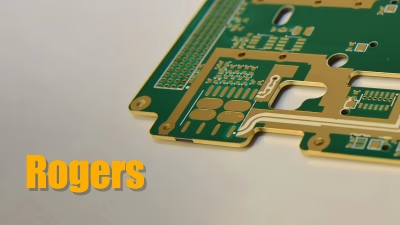
Rogers Corporation is an industry leader when it comes to high-frequency laminates, offering products such as the RO4000® series that balance performance with manufacturability.
- Pros: They come with various Dk values to offer designers more design freedom. Their hydrocarbon/ceramic blend provides low loss, great thermal stability, and efficient heat conduction. Crucially, they can often be processed using similar methods as FR-4 to drastically cut manufacturing cost and time, making them the ideal choice for many commercial products.
3.3 Ceramic Substrates and Filled Composites

These include materials such as Alumina (Al₂O₃), Aluminum Nitride (AlN) or Low Temperature Co-Fired Ceramic (LTCC).
- Pros: They possess superior thermal conductivity (especially AlN), making them suitable for high-power applications. Furthermore, their rigidity provides unrivalled dimensional stability while Dk remains constant across frequencies and temperatures.
- Application Areas:utilise in power amplifiers, RF modules, aerospace/military applications where performance and reliability are of utmost importance
4. Design Challenges and Engineering Solutions

Designing a high-frequency PCB requires extensive knowledge of electromagnetic fields, transmission line theory and thermal management.
4.1 Impedance Control
At the core of any high-frequency design lies Impedance Control. Transmission lines (such as microstrip or strip line ) must have an impedance characteristic matched to their source and load impedance (usually 50Ωor 75Ω). Any mismatch results in signal reflections that cause ringing, overshoot, and logic errors that require precise control over trace width, dielectric thickness and Dk (Dark Karma).
4.2 Signal Integrity (SI) Management
- Loss: Conductor and dielectric losses must be minimized to keep critical traces short, with designers choosing smooth copper materials with low dielectric loss factors to ensure conductivity while keeping critical traces as short as possible.
- Crosstalk:Crosstalk is unwanted coupling between adjacent signal traces that is minimized through increased spacing, ground plane shields, or differential pair routing. –
- Jitter and Phase Noise:For digital and RF systems operating at high speed, timing precision (jitter) and signal purity (phase noise) are both vital elements. Poor SI can drastically exacerbate either.
4.3 Electromagnetic Compatibility (EMC)
High-frequency circuits can be powerful sources of electromagnetic interference (EMI). Careful planning, the use of shields, continuous return paths and adding filters is necessary in order to avoid devices interfering with each other and disrupting signal flow.
4.4 Thermal Management
Heat is one of the primary causes of failure in electronics, so High-Frequency PCBs often employ thermal simulation to plan component placement and thermal vias (small copper-filled holes) help transfer heat away from components to heat sinks or enclosures for dissipation. High thermal conductivity substrates may also be chosen in order to avoid overheating issues.
4.5 Manufacturing Tolerances and Consistency
High-frequency circuits can be sensitive to physical dimensions; even minor adjustments in thickness or trace width can dramatically change impedance levels, necessitating close cooperation with PCB manufacturers so their processes meet design specifications precisely.
5. Applications — From the Cloud to the Sky
High-Frequency PCBs have become essential tools in many cutting-edge fields, from robotics and medicine to aerospace and healthcare.

5.1 Communication Networks
- 5G/6G Infrastructure: Massive MIMO antennas, Active Antenna Units (AAUs), and base stations which handle millimeter-wave signals are some of the primary users of High-Frequency PCBs.
- Satellite Communication: Low-Earth Orbit Internet satellites such as Starlink require reliable data links in harsh environments.
5.2 Automotive Electronics
- ADAS(Advanced Driver-Assistance Systems): The 77 GHz automotive radar used by self-driving cars serves as their “eye”, requiring exceptional frequency and phase stability in its core PCB.
- V2X (Vehicle-to-Everything): Future connected cars will use High Frequency PCBs to connect to other cars, infrastructure and the cloud.
5.3 Aerospace & Defense
- Radar Systems: The performance and range of radar, from aircraft systems to ground-based arrays, depend heavily on the low-loss and power handling capacities of their PCBs.
- Electronic Warfare (EW) Systems: EW systems utilize sophisticated RF circuits that can quickly tune across wide frequency bands.
- High-End Test & Measurement Equipment: Spectrum analyzers and network analyzers need to use High Frequency PCBs with superior performance for accurate measurements.
5.4 Medical Electronics
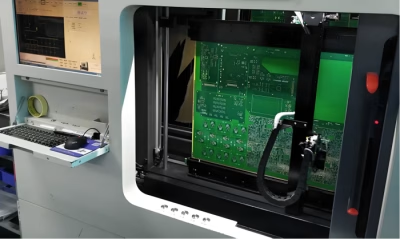
- Magnetic Resonance Imaging (MRI) :Systems requiring excitation and reception coils require high-performance PCBs in order to function optimally.
- Medical Microwave Ablation: Probes used to precisely destroy cancer cells employ circuits that control high-frequency energy.
6. Future Trends
As technology progresses, High-Frequency PCBs are evolving along several key directions:
- Integration and Modularization:When combined, antennas, passive components (resistors, capacitors and inductors), and active chips are directly embedded onto a PCB creating Antenna-in-Package (AiP) or Embedded Component PCBs which save space, improve performance, and lower assembly cost significantly.
- Continuous Material Innovation: Researchers continue their search for new composite materials with lower Dk/Df ratios, improved thermal conductivity, easier processing methods and lower costs. Materials like modified polyimide and Liquid Crystal Polymer (LCP) offer great promise as flexible high-frequency circuit components.
- Integration with Semiconductor Technology:Integration of Monolithic Microwave Integrated Circuits (MMICs) constructed from silicon, gallium nitride (GaN), or silicon carbide (SiC) materials with High Frequency PCBs has become the go-to way of increasing frequencies and widening bandwidths.
- AI and Machine Learning as Design Tools: Artificial Intelligence (AI) and Machine Learning will become essential tools in meeting increasingly complex design challenges. AI/ML solutions may assist with optimizing circuits, predicting failures and increasing manufacturing yield.
7. F&Q
The primary difference lies in the base material. Standard PCBs employ FR-4, with its high and unstable Dk and Df, while high-frequency boards use special materials like PTFE or Rogers laminates which have very stable Dk and very low Df, to meet the stringent demands of high frequency signals.
Three main reasons come into play here. These include (1) Material Cost – the special high frequency materials cost many times more than their FR-4 equivalent; 2) Processing Costs: These boards require special equipment and techniques (like plasma treatment) with tighter quality control procedures; and (3) Design Costs which necessitate expensive simulation software along with experienced RF engineers, lengthening design cycles further.
Nope. While lower Dk values can help with signal speed and crosstalk reduction, sometimes specific values are needed, for instance to create small antennas or high-value capacitors on PCB boards – choosing the appropriate Dk is more crucial than just choosing the cheapest value!
Impedance control involves designing PCB traces and material with a specific characteristic impedance (50Ω). If that impedance doesn’t match components properly, signals reflect back compromising signal quality, leading to errors, power losses and distorting waveforms – all detrimental effects that compromise signal integrity.
Longer traces incur more signal loss (insertion loss) and phase error, while sharp bends, such as 90-degree angles, alter transmission line properties causing impedance changes and signal reflections. Therefore, for optimal high frequency paths use curves or 45 degree angles in critical paths to avoid unnecessary signal loss or reflections.
Yes. This configuration is known as a hybrid or mixed dielectric stack-up and often features high frequency material for signal layers while digital and power layers use FR-4 material instead. Unfortunately, doing this poses some unique challenges because different materials expand at differing rates when heated causing reliability issues while impedance calculation becomes more complicated as well as more skilled manufacturers may need to be engaged for optimal results.
When designed correctly with high quality materials and manufacturing processes in mind, high frequency PCBs can be highly reliable – their use in demanding fields such as aerospace and automotive production environments where long life and stability are of great importance stands as proof.
Three key areas include 1) 6G Communication: Moving into Terahertz range will put materials and processes to the ultimate test; 2) L4/L5 Autonomous Driving will require higher-resolution, longer range imaging radar for autonomous driving systems; and 3) Low Earth Orbit Satellite Internet will require millions of low-cost, high performance user terminals equipped with phased array antennas which rely directly on High Frequency PCB manufacturing scale and cost.
8. Summary
High-Frequency PCBs represent the cutting-edge of modern electronics. Their role has far outshone that of simply connecting components, becoming complex electromagnetic platforms which set performance boundaries for system performance ranging from 5G speeds and self-driving car intelligence, space exploration feats to safeguarding human health; High-Frequency PCBs serve as essential “roadbeds and bridges” of our information highways.
If you’re looking for a reliable, cost-effective option that specializes in high frequency PCB manufacturers, check out Orinew Technology, With over 14 years of experience in PCB manufacturing and PCB assembly.








