
RF PCB: A Guide to Design, Materials, and Manufacturing Processes

Table of Content
Radio Frequency Printed Circuit Boards (RF PCBs) are the invisible backbone of modern wireless communication, directly determining the signal quality in everything from smartphones to radar systems. Unlike standard PCBs handling low-frequency signals, RF PCBs manage electromagnetic waves ranging from hundreds of MHz to tens of GHz. At these frequencies, a simple copper trace acts as a transmission line with distributed parameters. Minor oversights in material selection, layout routing, or impedance control can lead to severe signal distortion or system failure. This article provides a technical reference covering the definition of RF PCBs, core material requirements, critical design considerations and common pitfalls, and precise manufacturing processes. It also clarifies the distinctions between RF, microwave, and high-frequency PCBs before summarizing their wide-ranging applications.
1. What is an RF PCB?

An RF PCB (Radio Frequency Printed Circuit Board) is designed to handle high-frequency signals from 300 KHz to 300 GHz. Unlike standard PCBs where signals flow as electrical current, RF signals propagate as electromagnetic waves along transmission lines.
RF PCBs typically feature a characteristic impedance of 50 ohms. The core design goals are to minimize signal loss, ensure signal integrity, and control impedance. This requires treating traces as transmission lines—such as microstrip, stripline, or coplanar waveguide. Designers must manage phenomena like reflection, crosstalk, the skin effect, and dielectric loss. In essence, RF PCB design is a precision discipline centered on controlling high-frequency waves on a compact substrate.
2. Materials Used in RF PCB

The substrate material is the cornerstone of RF PCB performance. High-frequency signals are extremely sensitive to the dielectric properties of the base material. A poor choice can lead to severe signal degradation. At frequencies above 1 GHz, standard FR-4 material exhibits a relatively high Dielectric Constant (Dk) and Dissipation Factor (Df). This results in significant signal propagation delay and energy loss dissipated as heat.
Based on industry design experience, RF PCB material selection must focus on the following parameters:
- Dielectric Constant (Dk): Select materials with Dk < 4. The Dk must remain stableacross the entire operating frequency band. A lower Dk allows for faster signal propagation. The less the Dk varies with frequency and temperature, the better the phase stability.
- Dissipation Factor (Df or Tan δ): The smaller this value, the lower the signal attenuation. High-frequency applications, such as millimeter-wave, require extremely low Df values, typically ranging from 0.0022 to 0.0095.
- Coefficient of Thermal Expansion (CTE): RF circuits often involve power amplification, which generates significant heat. The CTE of the substrate should closely match that of the copper foil to prevent mechanical stress and failure during thermal cycling.
- Moisture Absorption: Low moisture absorption prevents the dielectric properties from drifting in humid environments.
Common Material Categories:
- PTFE (Polytetrafluoroethylene)-Based Materials: Such as the RO3000 and RO4000 series from major manufacturers and their equivalents. This is the gold standardfor RF PCBs. They offer very low Dk and Df with excellent high-frequency performance. However, they are softer materials, making them more difficult and costly to process.
- Hydrocarbon Ceramic Laminates: Models like RO4350B achieve a good balance between high-frequency performance and manufacturability. They are compatible with standard FR-4 processing flows and offer excellent cost-effectiveness.
- Ceramic-Filled Substrates: These are ideal for very high-power or high-heat-dissipation scenarios due to their excellent thermal conductivity.
- FR-4:This is only recommended for non-critical applications below 1 GHz. Using FR-4 above 5 GHz is a major error in RF design, leading to unacceptable insertion loss.
3. Design Considerations for RF PCB: Core Principles and Avoiding Common Mistakes

This section is critical to the success of any RF PCB. By analyzing common industry layout errors and professional design guidelines, we have distilled the design considerations into six core dimensions. We highlight frequent mistakes made by engineers and provide methods for correction and avoidance.
3.1 Impedance Control and Transmission Line Design
Consideration: RF signal paths must be treated as transmission lines. The characteristic impedance (typically 50Ω) must remain consistent from the source to the load. Any impedance discontinuity will cause signal reflections, degrading the return loss (S11) and reducing transmission efficiency.
Common Mistakes and How to Avoid Them:
- Mistake: Lack of impedance calculation. Setting RF trace widths arbitrarily without calculation.
Correction: Always use an impedance calculator tool. Precisely determine trace width based on the specific layer stack-up details, including prepreg thickness, copper weight, and substrate Dk value.
- Mistake: Sudden changes in trace widthor using 90-degree right-angle corners. This causes localized electric field concentration and effective width variation, creating impedance discontinuities.
Correction: Maintain consistent trace width along the RF path. When bends are necessary, use curved bends with a radius at least three times the trace width or use 45-degree mitered corners.
- Mistake: Excessive use of viasfor layer transitions. Each via introduces parasitic inductance (approximately 1 nH) and sub-picofarad capacitance. At GHz frequencies, this is sufficient to disrupt impedance matching.
Correction: Route RF traces on the top layer whenever possible. If a layer change is unavoidable, place accompanying ground vias immediately adjacent to the signal via. This provides a low-impedance return path for the signal current.
3.2 Grounding Design and Return Path Control
Consideration: High-frequency return currents always follow the path of least inductance. This path is the continuous reference ground plane directly beneath the signal trace. An incomplete ground plane forces the return current to detour, creating a “slot antenna” effect that causes EMI and crosstalk.
Common Mistakes and How to Avoid Them:
- Mistake: Discontinuous ground planecut by other traces, vias, or slots.
Correction: Ensure there is a solid, unbroken copper ground plane directly under all RF traces.
- Mistake: Isolated ground copper pours(floating copper) on the top layer. These areas are neither connected to the main ground nor stitched with sufficient vias.
Correction: Fill all empty areas with grounded copper. Stitch this copper to the inner main ground plane with a dense array of ground vias. The spacing should be between λ/20 and λ/10 (where λ is the wavelength at the operating frequency). For example, at 2.5 GHz, via spacing should be no more than 6 mm.
- Mistake: Sharing ground vias. Connecting multiple shunt components to ground through a single trace and via.
Correction: Each ground pad must have its own dedicated ground via to minimize parasitic inductance.
3.3 Power Supply Decoupling and Noise Isolation
Consideration: RF chips are highly sensitive to power supply noise. This is especially true for Voltage-Controlled Oscillators (VCOs) and Phase-Locked Loops (PLLs), where power supply ripple directly translates into phase noise.
Common Mistakes and How to Avoid Them:
- Mistake: Decoupling capacitors placed far from power pinsor arranged in a messy layout.
Correction: Follow the principle of “smaller capacitor closest.” Place the smallest value, high-frequency capacitors (e.g., 100 pF, 0.1 µF) as close as physically possible to the chip’s power pins. Larger bulk capacitors (e.g., 10 µF) can be placed slightly further away for energy storage and low-frequency filtering.
- Mistake: Mixing RF traces with digital or power circuits. Digital switching noise or DC-DC converter ripple can couple directly into sensitive RF receiver chains, desensitizing the receiver.
Correction: Use physical partitioning. Strictly separate the RF, digital, and power sections on the board layout. Use ground via fences or metal shielding cans to isolate these sections. Include pi-filter networks at the main power entry points.
3.4 Matching Network and Antenna Layout
Consideration: The matching network between the antenna and the RF chip, whether a pi-network or T-network, determines how efficiently energy is radiated. The electromagnetic field environment around the antenna is extremely sensitive and directly affects resonant frequency and radiation efficiency.
Common Mistakes and How to Avoid Them:
- Mistake: Matching network located far from the device pins, separated by a long 50Ω trace. This trace segment introduces additional parasitic inductance and phase delay, rendering the theoretical matching values ineffective.
Correction: Place matching components as close as possible to the RF chip pins or the antenna feed point. Keep the network compact.
- Mistake: Traces or copper pours located within the antenna keep-out area. Any metal object near the antenna will disturb the radiation field. This causes resonant frequency shifts and severely reduces efficiency.
Correction: Strictly adhere to the keep-out area specified in the antenna datasheet. Do not route traces, pour copper, or place components on any layer within this zone, including bottom and inner layers.
3.5 Stack-Up Design and Routing Strategy
Consideration: A well-designed layer stack-up provides a stable reference plane for signals, controls impedance, and isolates interference.
Common Mistakes and How to Avoid Them:
- Mistake: Using an asymmetrical stack-upor using a 2-layer board for a complex RF design. Two-layer boards lack dedicated power and ground planes, leading to long and uncontrolled ground return paths.
Correction: Use a 4-layer or higher stack-up as a minimum. A recommended structure is: Layer 1 (RF Signals & Components) – Layer 2 (Solid Ground Plane) – Layer 3 (Power Plane) – Layer 4 (Digital/Control Signals). Placing the ground plane directly adjacent to the RF layer provides the optimal return path and isolation. Maintain symmetry around the center of the stack-up to prevent board warpage.
- Mistake: Keeping solder mask on RF tracesin extremely high-frequency or ultra-low-loss applications.
Correction: For millimeter-wave or ultra-low-loss designs, remove the solder mask from the top of the RF traces. Solder mask has a higher Dk that is difficult to control precisely, and it adds a small amount of loss.
3.6 Thermal Management
Consideration: RF power amplifiers (PAs) are not 100% efficient. A significant amount of energy is dissipated as heat. High temperatures can alter the Dk of the substrate, causing impedance drift and frequency detuning. Heat also shortens component lifespan.
Common Mistakes and How to Avoid Them:
- Mistake: Neglecting thermal design for the PA area, relying solely on the component’s bottom pad for natural convection cooling.
Correction: Design a dense array of thermal vias under the PA’s ground/thermal pad. These vias conduct heat down to a large ground plane on the bottom layer or a metal heatsink. Industry practice suggests using vias filled with thermally conductive epoxy or embedding copper coins directly into the board to enhance vertical thermal transfer.
4. Manufacturing Processes for RF PCB
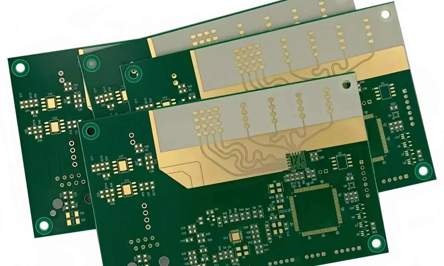
The manufacturing flow for RF PCBs is similar to that of standard PCBs, but the requirements for precision and material handling are far more stringent. Industry sources indicate that inter-layer alignment accuracy and etching precision are two major challenges in high-frequency board fabrication.
- Inner Layer Imaging and Etching: Because trace width is critical for impedance control, the amount of etch undercut must be strictly minimized. Line width tolerances are typically held to ±10% or better. Some processes use smoother reverse-treated copper foilsto reduce conductor loss caused by the skin effect at high frequencies.
- Lamination: Laminating high-frequency materials, especially PTFE, differs from processing standard FR-4. PTFE molecules are inert and difficult to bond. Plasma treatmentor the use of special bonding films is often required before lamination to ensure interlayer adhesion and prevent delamination.
- Drilling and Plating: Hole wall roughness directly impacts via parasitic parameters. Mechanical drilling must be followed by desmearand etchback For PTFE substrates, specialized plasma etching is used to clean the hole walls and ensure reliable electroless copper deposition. Controlling the shelf life of materials—for instance, storing high-frequency laminates for no more than 45 days—is an important manufacturing control step to prevent oxidation and moisture absorption, ensuring batch-to-batch consistency.
- Solder Mask and Surface Finish: As mentioned earlier, high-frequency microstrip lines often require solder mask clearance. The surface finish of choice is typically Electroless Nickel Immersion Gold (ENIG)or Immersion Silver. These finishes are very flat, minimizing impact on signal phase. It is important to be aware of potential “black pad” defects with ENIG, which can negatively affect high-frequency performance.
5. RF PCB vs. Microwave PCB vs. High-Frequency PCB
These three terms are often used interchangeably, but a subtle hierarchical relationship exists.
| Characteristic | High-Frequency PCB | RF PCB | Microwave PCB |
| Definition | A general term for PCBs operating above 10 KHz. | Specifically refers to PCBs operating in the Radio Frequency range (300 KHz – 300 GHz). | Specifically refers to PCBs operating in the Microwave band (300 MHz – 300 GHz). |
| Frequency Range | Broadest (includes RF and Microwave). | Intermediate. | Subset of high frequency (decimeter, centimeter, millimeter waves). |
| Typical Impedance | 50Ω, 75Ω, 100Ω, etc. | Typically 50Ω. | 50Ω or 75Ω. |
| Material Focus | May include modified FR-4. | Primarily uses PTFE/hydrocarbon ceramic laminates. | Most stringent Dk/Df requirements. Often uses top-grade PTFE or ceramic substrates. |
| Sensitivity to Physical Dimensions | Moderate. | High. | Extremely High (very short wavelengths make small structural changes significant). |
Conclusion: High-Frequency PCB is the broad general category. RF PCB is the specific subset focused on radio transmission and reception. Microwave PCB is the subset of RF PCB with the highest frequencies and greatest design difficulty.
6. Applications of RF PCBs

RF PCB technology is the cornerstone of a wirelessly connected world. Its applications permeate every facet of modern life:
- Wireless Communication Infrastructure: Antennas, filters, and power amplifier modules in 5G base stations, small cells, repeaters, and distributed antenna systems.
- Satellite and Aerospace: Satellite transceivers, synthetic aperture radar (SAR), and GPS/GNSS receivers.
- Automotive Electronics: 77 GHz millimeter-wave collision avoidance radar, V2X communication modules, and tire pressure monitoring systems.
- Consumer Electronics: Smartphones (integrating Wi-Fi 6E, Bluetooth, UWB, 5G NR modules), wireless routers, and smartwatches.
- Medical Devices: MRI RF coils, microwave ablation therapy instruments, and wireless endoscopes.
- Defense and Military: Phased array radar T/R modules, electronic countermeasure equipment, and secure communication systems.
7. FAQs
(1) Why are RF PCBs typically designed with a 50-ohm impedance?
This value is an engineering compromise that balances power handling capability and signal attenuation. In coaxial cables, the minimum loss for an air dielectric occurs at 77 ohms, while the maximum power handling occurs at 30 ohms. 50 ohms is the geometric mean and provides the optimal balance between these two factors. It later became the industry standard.
(2) Is a continuous ground plane under RF traces absolutely necessary?
Yes, this is crucial for signal integrity. The ground plane provides the lowest impedance return path for the RF signal. It also confines the electromagnetic field, preventing energy radiation and interference with other circuits. A discontinuous ground is one of the primary causes of poor RF performance.
(3) Can I use an FR-4 board for a 2.4 GHz Wi-Fi application?
For simple 2.4 GHz antenna feeds or very short traces, it might be marginally acceptable, but performance will not be optimal. The Dk variation and higher Df of FR-4 introduce extra loss and phase error. For products requiring high receiver sensitivity or complex modulation schemes like 802.11n/ac, it is strongly recommended to use a professional high-frequency laminate.
(4) What is the most easily overlooked detail in RF design?
The most easily overlooked detail is grounding, specifically the number and placement of ground vias. Many engineers focus exclusively on the signal trace itself. They forget to provide a clean, wide, and unobstructed path for the return current. Another common oversight is the clearance around the antenna.
8. Summary
RF PCB design combines electromagnetic theory, materials science, and precision manufacturing. Success depends on meticulous attention to detail—selecting low-loss substrates, enforcing strict impedance control, creating continuous ground return paths, optimizing decoupling, and isolating noise sources. Common layout errors usually stem from misunderstanding the distributed nature of high-frequency signals. By recognizing that signals travel as electromagnetic waves and using simulation tools early, engineers can avoid these pitfalls and produce stable, high-performance boards. With the expansion of 5G millimeter-wave, automotive radar, and satellite communications, mastering RF PCB design is now essential for hardware engineers.








