Power Management Unit (PMU) PCB Design Guide

Table of Content
- 1. Define the PMU functions and the rail requirements
- 2. Identify the switching loops before placing components
- 3. Route power, sensing and ground with different objectives
- 4. Select capacitors and inductors by operating conditions
- 5. Design the thermal pad and assembly process together
- 6. Separate design verification from production acceptance
- 7. Example: releasing two power-board variants
- 8. Prepare the PMU board for a turnkey PCBA quotation
- 9. PMU PCB design FAQ
PMU PCB DESIGN · LAYOUT, POWER INTEGRITY & ASSEMBLY RELEASE
Quick answer: Start PMU PCB design with a rail and power-sequence specification, then follow the exact regulator or PMIC hardware guidance. Review the DC delivery path, topology-specific switching-current loops, switch nodes and feedback routing separately. Select capacitors and inductors for their actual operating conditions, agree the stack-up and thermal-pad construction, and release a measurable acceptance plan with the BOM and assembly data. A generic trace-width formula or a working unloaded prototype cannot establish production readiness.
This guide answers a practical engineering question: what should be reviewed before a power-management board is released for PCB fabrication and assembly? It preserves the design focus while connecting electrical decisions to the parts, manufacturing details and tests a supplier needs to quote and build the board.
For a project review, send your current files and quantities to our turnkey PCBA and BOM quotation page. Identify unresolved power, thermal and test requirements rather than asking the assembler to infer them from a schematic image.
1. Define the PMU functions and the rail requirements
A power management unit, or PMU, is the power-management function or subsystem in a product. A power management IC, or PMIC, implements a particular set of functions in an integrated circuit. Product terminology varies: inspect the exact part rather than assuming a PMU always includes a charger, fuel gauge, every protection function or seamless source switching.
The implementation may combine buck, boost or buck-boost converters, LDOs, load switches, monitoring and sequencing. Choose these around the load and operating states. If a processor requires a particular start-up sequence or voltage setting, release that requirement along with the actual PMIC configuration and ordering option.
| Requirement | Specify | Review question |
|---|---|---|
| Input conditions | Normal supply range, intended sources, transients and required protection. | Are components and behavior suitable for the actual operating and abnormal conditions? |
| Each output rail | Voltage, tolerance, steady/transient load, allowed ripple and operating states. | Where and how is each requirement measured? |
| Sequence and control | Enable, reset, power-good, ramp, shutdown, configuration and firmware dependencies. | What must happen before the next rail or load can start? |
| Physical environment | Board and enclosure limits, ambient conditions, cooling and interfaces. | Does the thermal assessment represent the assembled product? |
| Acceptance scope | Prototype characterization versus repeatable production checks and records. | Which evidence is required for each shipped assembly? |
Keep these requirements separate from a component’s absolute maximum ratings. Operation inside an absolute maximum limit does not, by itself, establish correct regulation or a reliable operating point.
2. Identify the switching loops before placing components
Switching-current loops depend on the converter topology and the states of its switches. Identify the paths whose current changes rapidly during a transition; do not assume the same loop dominates a buck, boost and buck-boost stage. Review the selected device’s reference circuit and layout with its actual package and operating mode.
Place the critical local capacitors and switching components to control those paths. A short-looking connection is insufficient if its return makes a large loop. Consider the full outgoing and return paths, including layer transitions and package connections.
Review switch-node copper separately from the DC output path. Unnecessary switch-node area can increase coupling, while an inadequate connection can create electrical or thermal problems. Follow device-specific guidance for copper beneath the node, adjacent planes and any keep-outs; neither a mandatory plane directly underneath nor a mandatory void is a universal PMU rule.
Keep sensitive feedback and control routing away from switching nodes and the associated interference paths. Review the inductor’s construction and orientation, nearby circuitry and actual coupling. Rotating every adjacent inductor by 90 degrees is not a substitute for evaluating the selected magnetic components and the layout.
3. Route power, sensing and ground with different objectives
The main DC path must meet voltage-drop and thermal requirements. Evaluate copper thickness, width, length, layer placement, allowable temperature rise, vias and connection bottlenecks. A rule such as “current multiplied by a fixed number of mils” ignores too much of the board construction to serve as a universal design limit.
Use a suitable calculation or validated design method, state its assumptions, and confirm the critical operating conditions. Power and return vias do not need numerically identical counts as a general rule. Their capacity, position and the resulting loop geometry matter more than matching two numbers.
| Decision | Check in the design | Avoid this shortcut |
|---|---|---|
| DC current delivery | Voltage drop, heating, copper geometry, vias and connector bottlenecks. | One trace width or one amp-per-via rule for every construction. |
| Switching-current loop | The topology, transition path, local components and return connection. | Looking only at the length of the positive supply trace. |
| Feedback / remote sense | The specified sensing point, reference connection, noise exposure and routing. | Sensing at a convenient point that does not represent the intended load voltage. |
| AGND / PGND | The exact pin functions, recommended connections and uninterrupted required return paths. | Splitting every ground plane or always joining grounds under the pad. |
| Layers and transitions | Reference continuity, routing access, copper distribution and thermal paths. | Copying a four-layer diagram without checking the real stack-up and currents. |
Analog and power ground names describe functions; they do not establish one connection pattern for all ICs. Some parts require a particular local connection, while other implementations rely on a continuous plane. Preserve the manufacturer’s intended grounding arrangement and avoid forcing sensitive return current through a noisy path.
Agree the real stack-up with the fabricator. A top-signal/ground/power/bottom-signal arrangement can be a starting discussion, not a guarantee of shielding, thermal performance or EMI compliance. Plane spacing, copper geometry and the routes’ reference paths remain part of the review. See our PCB manufacturing service for the fabrication handoff.
4. Select capacitors and inductors by operating conditions
A capacitor’s nominal capacitance is only a starting point. For an LDO or converter, check the required effective capacitance, ESR range where applicable, voltage and temperature behavior, tolerance and the permitted placement. Ceramic DC-bias effects can make the operating capacitance substantially different from the printed value.
Do not assume every LDO is stable with any low-ESR ceramic capacitor. Its architecture and data sheet determine the acceptable network. Likewise, a ceramic dielectric designation alone does not establish that a proposed replacement is equivalent.
For inductors, review the required inductance, saturation and thermal-current ratings under the manufacturer’s stated test definitions, DCR, losses, package, shielding and temperature limits. A similar value and footprint do not prove that two parts behave alike in the converter.
- Release exact manufacturer part numbers and the actual package/order options.
- Identify approved alternatives separately from candidates awaiting engineering approval.
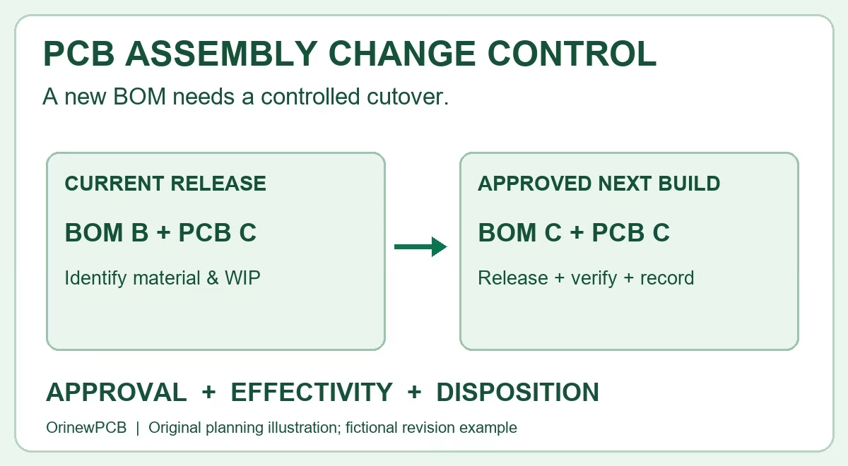
- Recheck effective capacitance, magnetic behavior, thermal limits and mechanical fit after a sourcing change.
- Keep configuration, feedback components and variant/DNP instructions aligned with the released rail requirements.
For purchasing approval, use our approved manufacturer list and BOM alternatives checklist. A lower price is useful only when the offered component remains appropriate for the approved design.
5. Design the thermal pad and assembly process together
Estimate losses for the intended operating states and identify how heat leaves the devices. The exposed pad’s electrical connection is device-specific: verify whether it belongs to ground, a power node or another defined connection before assigning its copper.
Agree the land pattern, solder-mask and stencil treatment, thermal-via geometry, via filling/capping or other necessary process details with the fabricator and assembler. Open vias in a soldered area may affect solder distribution; adding more holes without reviewing the assembly process is not a complete thermal solution.
Compare calculations with the real board and enclosure conditions. Package thermal metrics depend on their definition and test setup. Do not treat a data-sheet junction-to-ambient number as a universal property independent of the PCB.
A thermal camera measures a surface condition, not junction temperature directly. A nearby NTC also measures its local thermal condition. Use an appropriate device-specific method to estimate or measure the relevant temperature, and record ambient conditions, load, cooling, operating mode and stabilization criteria. Placing a PMU near an exhaust vent is not automatically the best choice when that air has already been heated by other devices.
Keep component accessibility, rework constraints and the required inspection method in the assembly review. For obscured joints, discuss suitable inspection coverage rather than assuming an external visual image establishes the entire pad connection.
6. Separate design verification from production acceptance
Before first power-up, review assembly identity, polarity, shorts checks and the released setup. Use an approved bring-up procedure with suitable supply protection and measurement connections. Do not improvise destructive fault tests on production assemblies.
| Check | Release the conditions | Interpret the evidence |
|---|---|---|
| Rail voltage / ripple | Input and load states, measurement point, probe arrangement and bandwidth. | A voltage measured at one point and load does not characterize all rail behavior. |
| Sequence / start / stop | Input ramp, enables, configuration, load state, timing and reset/power-good criteria. | A successful boot does not prove every required sequence and shutdown condition. |
| Load response | Defined transient magnitude, edge conditions and allowed voltage excursion/recovery. | An unloaded bench demonstration is not a load-transient result. |
| Efficiency / temperature | Power measurement boundaries, load/input points, ambient and cooling state. | System current or surface temperature alone cannot establish every IC’s loss or junction temperature. |
| EMI / product evaluation | Required standard, setup, cables/enclosure, operating modes and responsible test activity. | A near-field scan locates possible sources; it does not certify compliance. |
Investigate excessive ripple or voltage droop using measured evidence: distinguish probe pickup, regulation behavior, current limiting, component selection, supply impedance and layout effects. Do not change capacitors or control modes simply to hide a symptom without checking stability and the operating requirements.
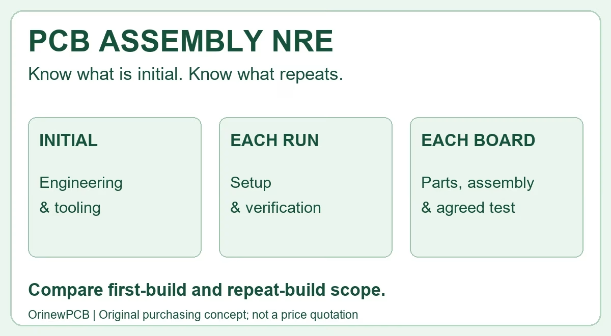
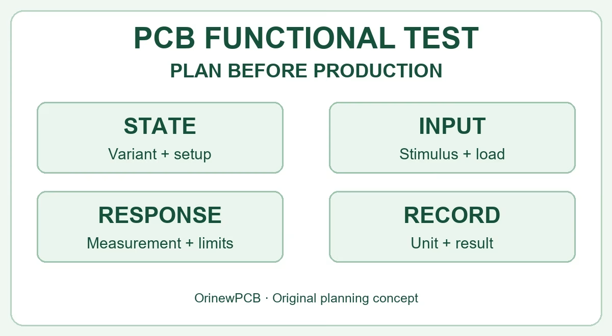
Production acceptance should identify the checks run on each agreed unit or lot, the limits, records and treatment of failures or rework. Use the PCBA functional test plan checklist to turn a requirement into a repeatable supplier instruction. Bare-board electrical testing and assembled-board functional testing provide different coverage.
7. Example: releasing two power-board variants
Illustrative planning example, not a customer project: a team orders a sensor-board variant and a higher-load controller variant that share one PCB. The BOM identifies the exact fitted converter, inductor, capacitors and feedback components for each. A release manifest connects those BOMs to the board files, assembly drawing, configuration and test-plan revisions.
The sensor version’s successful boot is not used as approval for the controller version. Engineering defines the controller’s load and thermal conditions, verifies that the fitted component choices remain suitable, and releases the required rail and sequence limits for that variant.
Before purchasing, the supplier flags a candidate capacitor replacement. The design owner reviews its effective capacitance and other relevant behavior, then records approval or rejection. That decision is reflected in the build package rather than accepted through an undocumented “same microfarads” substitution.
8. Prepare the PMU board for a turnkey PCBA quotation
A useful manufacturing quote brings the design, material and acceptance scope together. Send:
- Gerber/drill data, board outline and the requested material, stack-up, copper and special via/pad details.
- BOM with exact manufacturer/MPNs, placement data, assembly drawings, fitted/DNP variants and approved alternatives.
- Quantity per variant, prototype and repeat-order expectations, destination and requested delivery date.
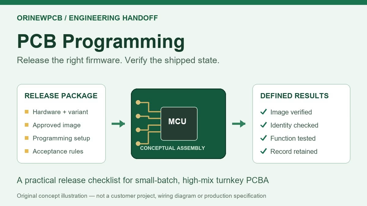
- Rail and sequence requirements, configuration/programming responsibility and unresolved design questions.
- Inspection and functional-test requirements, fixtures/loads, measurement limits and requested result records.
- Any customer-supplied components, traceability requirements and approvals still needed before procurement or production.
OrinewPCB provides PCB fabrication, component sourcing and turnkey PCB assembly, with particular strength in small/medium batches and high-mix projects. Our policy is to supply and assemble with 100% new, original and genuine electronic components. Cooperation with manufacturers and distributors supports BOM-specific sourcing; offered price, availability and delivery are confirmed for the actual order.
We emphasize quality through our nine-stage PCBA quality workflow and 100% flying-probe electrical testing of the bare PCBs we manufacture. Those checks have different purposes from a power board’s agreed rail, sequence and load tests. Specify the acceptance work your product needs when requesting a quotation.
Request a PMU Turnkey PCBA & BOM Review
For parts-only requirements, use our electronic components directory. The brand’s OrinewPCB assembly service overview explains the wider service scope.
9. PMU PCB design FAQ
Is a PMU the same as a PMIC?
Terminology varies. PMU can describe a product’s power-management function or subsystem, while PMIC identifies an integrated circuit implementing particular functions. Check the actual device and configuration; charging, fuel gauging or source switching are not automatically present in every part.
Should AGND and PGND always be separated?
No universal plane split or join location applies to every regulator. Follow the exact device’s recommended connections and review the actual current return paths. A copied split can interrupt a required return or couple noise into sensing.
Can I size a power trace using only its current?
No. Current is one input alongside copper thickness, width, length, layer environment, temperature rise, voltage drop and connections. Use a suitable calculation with explicit assumptions and verify critical operating conditions.
Can I replace an output capacitor with any part of the same value?
Not safely on that description alone. Check effective capacitance at the operating voltage and temperature, tolerance, ESR/ESL where relevant, ratings and the regulator’s stability requirements. Release an alternative through engineering approval.
Does a thermal image show the PMIC junction temperature?
It shows a measured surface condition under the instrument’s setup. Relating that to junction temperature needs an appropriate method and relevant device/system information. Record the actual load, ambient and cooling conditions.
Does flying-probe PCB testing prove that the PMU will work?
Bare-board electrical testing checks the unpopulated PCB against its agreed electrical scope. It does not verify installed components, configuration, rail sequencing, regulation, load response or the finished product’s compliance. Define the required assembly inspection and functional acceptance separately.
Application-dependent engineering guidance. Use current product documentation and approved design limits for the released hardware. Original concept figures and the example above are not manufacturing drawings or customer test results.
Related Posts
ORINEWPCB · PROJECT SUPPORT
Contact Us
Discuss your PCB assembly project with our team.
FREE QUOTE
Plan your turnkey PCBA build.
Share your quantity and requirements. Add Gerber files and a BOM when ready.
Files are optional for an initial discussion. Include any assembly, sourcing or testing requirements in your message.