Post-Reflow AOI: Defects, Limits & PCBA Inspection Checklist

Table of Content
Post-reflow AOI inspects the visible features of a PCB assembly after the solder paste has reflowed. Depending on the inspection system, program and viewing access, it can flag missing or displaced parts, polarity issues, visible solder bridges and abnormal solder-joint geometry. It does not establish electrical operation or reveal every hidden joint. For a turnkey PCBA order, agree the inspected features, acceptance criteria, review process and complementary tests before production.
This guide is for hardware engineers and buyers specifying inspection for an assembled board. Use it to review an inspection proposal, prepare a pilot build and clarify what an “AOI passed” result actually covers. For a wider introduction, see our automated optical inspection overview.
Planning a turnkey build? Send your files for an assembly and inspection quote.
1. Where post-reflow AOI fits in the SMT process
Post-reflow AOI is usually placed after the reflow oven and the handling or cooling arrangement required by the line. The board must be presented within the inspection equipment’s operating conditions. Its purpose is to inspect the assembly after solder joints have formed, rather than predict their final appearance from an unsoldered placement.
Earlier inspection has a different job. Solder paste inspection (SPI) examines deposited paste. Pre-reflow AOI examines placement before soldering. Those stages can provide useful upstream evidence when post-reflow inspection finds a recurring problem. Double-sided or mixed-technology assemblies need a plan for each relevant assembly stage; inspecting one side does not automatically cover the other side or later through-hole work.
2. What defects can post-reflow AOI detect?
Detection depends on whether the relevant feature is visible, whether the machine can measure it and whether the inspection recipe includes an appropriate check. “Detected by AOI” should describe a verified inspection capability for that board, not an unconditional promise.
On a phone, swipe the table horizontally. Keyboard users can focus the table region and use the arrow keys.
| Feature or concern | Potential AOI check | Important limitation or follow-up |
|---|---|---|
| Missing, shifted or rotated part | Compare the observed body, leads and position with the programmed package and orientation. | Confirm the correct package library, reference designator and board revision were used. |
| Polarity or visible marking | Inspect an accessible orientation mark or readable top marking when the program supports it. | Some parts have ambiguous or unreadable markings. Identical-looking parts can have different electrical values. |
| Solder bridge | Flag a visible connection between leads or pads where optical access is sufficient. | Hidden bridges beneath a package need an appropriate additional inspection or electrical check. |
| Lifted lead, tombstone or height anomaly | Inspect lead position, body posture or measured height; 3D measurement can add useful geometry. | Coverage still depends on package geometry, shadows, line of sight and the inspection recipe. |
| Insufficient or abnormal visible solder | Evaluate accessible solder shape or measured features against the agreed criteria. | Optical appearance alone does not prove internal joint integrity, alloy composition or electrical continuity. |
| Possible wrong component | Compare package and visible markings where they are distinguishable. | Use BOM controls, sourcing records and appropriate electrical testing for characteristics that cannot be identified optically. |
3. What an AOI pass does not prove
A camera-based inspection needs usable optical access. Many BGA joints, bottom-terminated connections and features obscured by adjacent components cannot be fully evaluated from above. A clean AOI result also does not demonstrate the correct resistor value, working firmware, power-rail behavior or operation under load.
Terms such as “cold solder joint” need care. AOI may flag a suspect visible shape or surface condition, but a visual classification alone cannot establish the underlying metallurgy or long-term reliability of a joint. The investigation and acceptance decision should follow the product requirements and supporting evidence.
Specify complementary coverage. Use X-ray inspection for selected hidden-joint concerns, suitable electrical testing for the accessible nets or components in its test program, and functional testing for defined operating behavior. Each method has limits. A complete test proposal should explain both included checks and known exclusions.
4. How to compare 2D AOI, 3D AOI and other inspection
- 2D AOI: uses image information such as location, color, contrast and visible shape. Its usefulness depends on lighting, viewing angles and the programmed checks.
- 3D AOI: adds surface-height or shape measurements that can help evaluate body posture, coplanarity and accessible solder geometry. It does not remove every shadow or make an optically hidden joint visible.
- X-ray inspection: provides information about selected internal or concealed structures. Confirm whether the proposed method is 2D transmission, angled viewing or CT and what defect criteria and coverage are included.
- Electrical and functional testing: answer different questions. Flying probe or ICT coverage depends on access and the test program; functional testing depends on supplied firmware, fixtures, operating conditions and pass/fail limits.
Ask the supplier to demonstrate coverage of your critical packages rather than choose only by the labels “2D” or “3D.” For electrical-access planning, use our PCB probe testing and test-point checklist. Keep optical inspection and product-function approval as separate, documented parts of your release plan.
5. A seven-point post-reflow AOI checklist for turnkey PCBA
- Release one controlled data set. Align the Gerber or manufacturing data, BOM, placement file, assembly drawing, polarity notes and do-not-populate list. State the board revision and both sides to be assembled.
- Identify high-consequence features. Highlight fine-pitch leads, polarized parts, densely packed connectors, hidden joints and parts with similar packages but different values. Ask how each will be verified.
- Define the inspected stage. State whether the scope covers each SMT side and what inspection follows any later through-hole soldering, rework or finishing. An earlier pass cannot automatically approve later work.
- Agree acceptance requirements. Identify the applicable standard, agreed revision, product class where relevant, and customer-specific requirements. Avoid an unspecified “IPC compliant” statement or a universal defect percentage copied from another product.
- Review programming on the pilot build. Confirm package libraries, reference positions, orientation checks, limits and example images for critical features. A known-good reference can assist programming but is not proof of all acceptance requirements.
- Define review and containment. Separate machine calls from confirmed defects. Identify who reviews suspect boards, how disposition is recorded, and how repeat defects trigger investigation of printing, placement or the measured reflow process.
- Control changes and retain agreed evidence. Review the inspection recipe after relevant BOM, package, layout or process changes. Specify the board or lot identification, results and reinspection records required with delivery.
OrinewPCB can review inspection and test requirements together with turnkey PCB assembly, PCB fabrication and BOM procurement. The inspection scope, documentation and commercial terms must be confirmed for the specific build.
6. Example: turn an AOI call into an engineering decision
Illustrative example, not a customer case: a pilot board repeatedly flags a fine-pitch lead at reference U12. Start by reviewing the recorded images and measurements against the agreed criteria. Determine whether this is a confirmed assembly defect, an imaging limitation or an overly sensitive program condition.
If it is a defect, contain the affected material and investigate the relevant upstream evidence, such as paste deposits, placement and the measured thermal profile. Approve any rework and repeat the required inspection or test. If it is a false call, document why the board is acceptable before changing the recipe, and check that the adjustment does not hide a real defect. Reducing the number of calls alone is not evidence of improved quality.
For thermal-process context, see our PCB preheating and profile verification guide.
7. See a real AOI station
The following short clip is from the official OrinewPCB channel. It illustrates an AOI station; it does not establish a particular program, detection rate, acceptance class or hidden-joint coverage for your order.
Watch the official AOI test clip on YouTube · OrinewPCB official channel
8. What to send for an inspection-ready PCBA quote
A useful quote should identify the manufacturing work, inspection coverage, complementary tests and records being purchased. Sending a board image and asking for “full AOI” leaves important decisions unresolved.
| Send or confirm | Useful information | Decision it supports |
|---|---|---|
| Build files and revision | Manufacturing files, BOM, placement data, assembly drawing and DNP notes. | Align fabrication, procurement, assembly and inspection to one released design. |
| Quantity and build stages | Pilot quantity, production quantity, populated sides and any later soldering or finishing. | Plan inspection programming, review effort and the relevant process stages. |
| Critical packages and features | BGA/QFN locations, fine-pitch leads, polarity notes, inaccessible areas and risk priorities. | Identify optical limits and where other inspection or test methods are required. |
| Acceptance requirements | Applicable standard and revision, agreed product class and customer-specific criteria. | Define pass/fail decisions before the pilot run. |
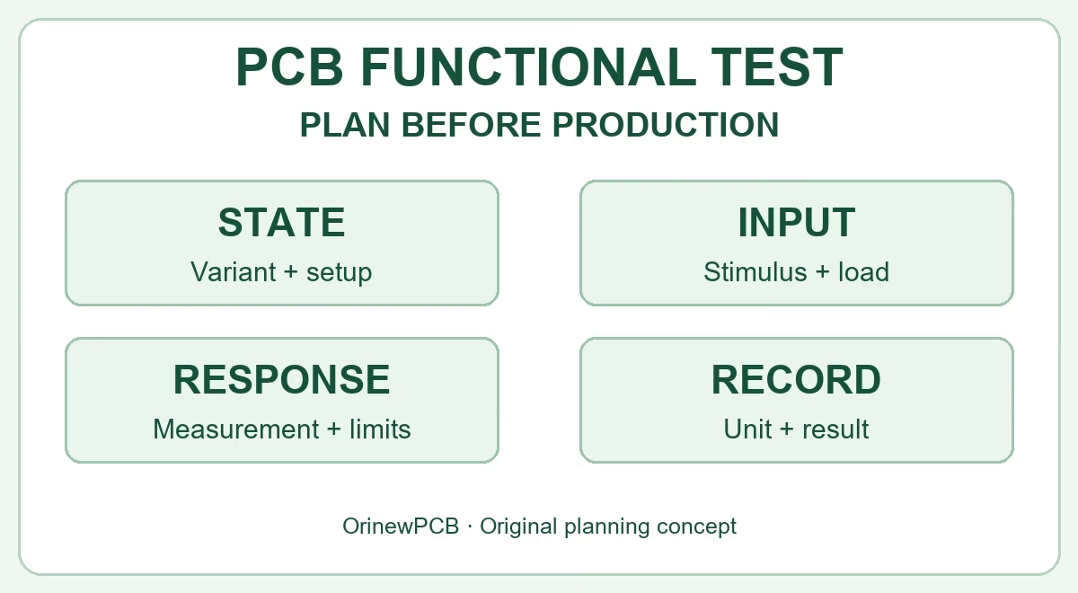
| Electrical or functional scope | Test points, intended checks, firmware version, interfaces, fixtures and operating limits. | Review feasible test coverage, exclusions and any tooling or programming work. |
| Reporting and traceability | Required lot/board identifiers, inspection records, defect images and rework/retest evidence. | Confirm what records are included and how repeat orders are controlled. |
| Material responsibility | Turnkey or supplied materials, approved part numbers and substitution-approval rules. | Coordinate component sourcing with package verification and the released BOM. |
Plan the build and inspection scope together
Send OrinewPCB your files, quantity and critical inspection requirements for a turnkey PCBA review. We can discuss PCB fabrication, component procurement, assembly and project-specific inspection or testing in one quotation.
OrinewPCB’s policy is to supply and assemble with 100% new, original genuine components. Approved manufacturer part numbers and any proposed alternatives should be confirmed before procurement or assembly. Component availability, price and delivery are confirmed for each quotation.
Need a narrower scope? Ask about PCB manufacturing or electronic component sourcing. You can also review the brand’s PCB assembly service scope.
9. Post-reflow AOI FAQ
What is post-reflow AOI?
It is automated optical inspection of a PCB assembly after reflow soldering. The inspection program evaluates selected visible component and solder features against defined criteria. Coverage depends on the board, equipment, optical access and recipe.
Is post-reflow AOI the same as SPI or pre-reflow AOI?
No. SPI inspects deposited solder paste, pre-reflow AOI examines placement before soldering, and post-reflow AOI examines the assembly after joints form. They provide different evidence and can complement one another.
Can AOI detect every wrong resistor or capacitor?
No. A package or readable marking may help identify a mismatch, but two parts can look the same while having different electrical values. Use approved BOM and sourcing controls plus suitable electrical verification where required.
Can 3D AOI inspect BGA joints underneath the package?
3D AOI measures optically accessible surfaces. A concealed BGA joint needs an appropriate complementary inspection or test plan. Define the actual X-ray and electrical coverage rather than assuming the word “3D” includes hidden joints.
Does an AOI pass mean the board works?
No. AOI does not power the circuit or verify the complete product’s behavior. Define functional testing, firmware, fixtures, operating conditions and pass/fail limits separately when those checks are required.
How should false calls be handled?
Review the suspect feature against the agreed acceptance requirements and supporting images or measurements. Document the disposition and validate any recipe adjustment. Avoid loosening limits simply to reduce review work.
Is AOI included in every turnkey PCBA quotation?
The inspection scope should be explicit in your quotation. Ask which stages, sides, features, complementary tests and reports are included. Product-specific requirements may need additional engineering, tooling or testing work.
What files should I send to OrinewPCB?
Start with your manufacturing files, BOM, placement data, assembly drawing, revision and quantities. Add critical packages, acceptance requirements, test needs and required records. Use the PCBA quote form to discuss the complete build.
Related Posts
ORINEWPCB · PROJECT SUPPORT
Contact Us
Discuss your PCB assembly project with our team.
FREE QUOTE
Plan your turnkey PCBA build.
Share your quantity and requirements. Add Gerber files and a BOM when ready.
Files are optional for an initial discussion. Include any assembly, sourcing or testing requirements in your message.