
Mastering Solder Ball Prevention in PCB Assembly

Table of Content
1. The Challenge of Solder Balls
In the intricate world of Surface Mount Technology(SMT) manufacturing and PCB assembly, achieving defect-free production is paramount. Among the myriad challenges, the formation of “solder balls” stands out as a persistent and often perplexing issue. These tiny, unwanted spheres of solder can severely compromise the reliability and functionality of electronic devices, leading to potential electrical shorts, reduced product lifespan, and costly rework or scrap.
This article delves deep into the phenomenon of solder balls, exploring their definition, significant impact, and, most importantly, the common causes and comprehensive strategies to prevent them. By understanding the root issues—ranging from solder paste properties and stencil design to reflow profiles and PCB layout—manufacturers can implement robust controls to ensure a smooth, high-quality PCB assembly process, ultimately enhancing product performance and reducing manufacturing costs.
2. What are Solder Balls and Why do They Matter?
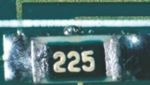
Solder balls are small, spherical deposits of solder that are typically found adjacent to solder joints on a printed circuit board(PCB) after the reflow soldering process. They are unintended byproducts and should not be confused with the controlled spherical shape of a properly formed solder joint. Their size can vary, but even microscopic solder balls can pose significant risks.
The Impact of Solder Balls
The presence of solder balls is more than just an aesthetic flaw; it indicates a process defect that can have serious implications:
- Electrical Shorts: The most critical concern is the potential for solder balls to bridge adjacent pads or traces, causing unintended electrical shorts. This can lead to device malfunction, catastrophic failure, or safety hazards.
- Reduced Reliability: Even if a solder ball doesn’t immediately cause a short, its presence signifies an unstable soldering process, which can lead to latent defects and reduced long-term reliability of the PCB.
- Cosmetic Defects: In high-visibility products, solder balls can be deemed unacceptable for their appearance, impacting brand perception.
- Costly Rework and Scrap: Detecting and removing solder balls often requires manual rework, which is time-consuming and expensive. In severe cases, entire boards may need to be scrapped, leading to significant material and production losses.
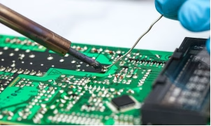
- Yield Reduction: A high incidence of solder balls directly impacts manufacturing yield, reducing the number of usable boards produced.
3. Common Causes of Solder Balls in SMT Production
Solder balls can originate from various stages of the SMT assembly process. Understanding these common causes is the first step toward effective prevention.
3.1 Solder Paste Related Issues
- Excessive Solder Paste: Applying too much solder paste through the stencil can lead to overflow during reflow, forming balls.
- Incorrect Solder Paste Viscosity: Paste that is too thin can slump, allowing solder particles to separate from the flux and form balls. If too thick, it can hinder proper release from the stencil.
- Paste Contamination or Degradation: Moisture absorption, expired paste, or contamination can alter paste properties, making it prone to spitting during reflow.
- Inadequate Metal Content: Solder paste with lower metal content may have higher flux volumes, which can push out solder particles.
- Improper Storage: Storing solder paste incorrectly (e.g., not refrigerated, exposing to humidity) can degrade its performance.
3.2 Stencil Design and Printing Problems
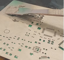
- Incorrect Aperture Design: Apertures that are too large or improperly shaped for the corresponding pad can deposit excessive paste.
- Poor Stencil Alignment: Misalignment between the stencil and the PCB pads can result in paste smearing and irregular deposits.
- Worn or Damaged Stencil: A worn stencil can lead to uneven paste deposits and bridging.
- Insufficient Stencil Cleaning: Solder paste residue on the bottom side of the stencil can smear and create paste bridges that become solder balls.
- Improper Squeegee Pressure or Speed: Too much pressure can cause paste to squeeze under the stencil; too little can result in incomplete fills.
3.3 Reflow Soldering Profile Issues
- Too Fast Ramp Rate: A rapid increase in temperature can cause the flux to volatilize too quickly, expelling solder particles outwards before they can coalesce.
- Insufficient Preheat: If the preheat zone is too short or the temperature too low, the flux may not be fully activated to clean the metal surfaces and remove oxides effectively.
- Incorrect Peak Temperature or Time Above Liquidus (TAL):Insufficient peak temperature can lead to poor wetting and incomplete coalescence, while excessively high temperatures can cause rapid flux evaporation.
- Improper Cooling Rate: Cooling too slowly can lead to excessive inter metallic growth, while too quickly can cause thermal shock.
- Oxidation: Excessive oxygen in the reflow oven can hinder the flux’s ability to clean metal surfaces, leading to poor wetting and solder ball formation.
3.4 PCB Design Considerations

- Solder Mask Defined (SMD) vs. Non-Solder Mask Defined (NSMD) Pads: Improperly designed SMD pads or inadequate solder mask dams between pads can create areas where solder paste can escape.
- Vias in Pads (VIP):If not properly tented or filled, vias in pads can wick away solder paste or flux, creating voids and potential solder ball sites.
- Pad Size and Spacing: Pads that are too large or too closely spaced can encourage bridging and solder ball formation.
- Surface Finish: Poor surface finish on pads can lead to inadequate wetting.
3.5 Component Placement and Handling
- Component Misalignment: Misplaced components can push solder paste outwards during reflow, creating balls.
- Component Warpage: Warped components may not sit flat on the board, leading to uneven pressure on the solder paste during reflow.
- Moisture Sensitive Components: Components not stored correctly can absorb moisture, which can out gas violently during reflow, spitting solder.
3.6 Environmental Factors
- High Humidity: Excessive humidity can affect solder paste properties, leading to moisture absorption and spitting during reflow.
- Dust and Contamination: Dust or debris on the PCB or in the solder paste can act as nucleation sites for solder balls.
4. Comprehensive Strategies to Avoid Solder Balls
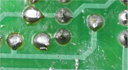
Preventing solder balls requires a multi-faceted approach, addressing each potential cause with specific mitigation techniques.
4.1 Solder Paste Management and Selection
- Optimize Paste Volume: Ensure stencil aperture designs match pad sizes and target solder volumes accurately. Use appropriate stencil thickness.
- Select Proper Solder Paste: Choose a paste with suitable viscosity, metal content, and flux activity for the specific application and components. Reputable suppliers often provide data sheets that guide proper usage.
- Strict Storage Protocols: Store solder paste under refrigeration, allowing it to reach room temperature gradually before use (typically 2-4 hours). Always reseal containers tightly.
- Maintain Freshness: Use solder paste within its recommended shelf life. Avoid using expired or degraded paste.
4.2 Stencil Design and Printing Process Optimization
- Precision Stencil Design: Collaborate with stencil manufacturers to ensure optimal aperture sizes and shapes, often slightly smaller than the pad for better definition. Consider step stencils for boards with varied component sizes.
- Regular Stencil Cleaning: Implement an automated stencil wipe system (dry, wet, or vacuum) to remove paste residue after each print or at regular intervals. Manually inspect and clean the stencil as needed.
- Optimized Print Parameters: Fine-tune squeegee pressure, speed, and separation speed to achieve consistent and precise paste deposition.
- Advanced Stencil Technologies: Consider electroformed stencils or those with specialized coatings (e.g., nano-coating) to improve paste release and reduce bridging.
4.3 Reflow Profile Tuning and Control
This is one of the most critical areas for solder ball prevention.
| Reflow Zone | Optimization Strategy | Benefit for Solder Ball Prevention |
| Preheat Zone | Ensure a gradual ramp rate (e.g., 1-2°C/second) and sufficient preheat time (e.g., 60-120 seconds) to allow flux activation and solvent evaporation. | Prevents rapid flux volatilization and ensures proper cleaning of oxides, allowing solder to coalesce smoothly. |
| Soak Zone(if applicable) | Maintain a steady temperature (e.g., 150-180°C) for a duration that allows temperature equalization across the board. | Further activates flux and reduces temperature differentials, minimizing component shock. |
| Reflow(Peak) Zone | Achieve the recommended peak temperature and time above liquidus (TAL) for the specific solder paste. Ensure components reach reflow temperature adequately. | Ensures complete melting and coalescence of solder particles, forming strong, consistent joints. Avoid s incomplete reflow. |
| Cooling Zone | Implement a controlled cooling rate (e.g., 2-5°C/second) to ensure proper solidification without inducing thermal stress. | Helps achieve proper grain structure and prevents issues like tombstoning, although less directly related to initial solder ball formation. |
4.4 PCB Design for Manufacturability(DFM)
- Solder Mask Design: Ensure proper solder mask dams between pads, especially for fine-pitch components. The solder mask should be well-defined and accurately registered.
- Pad Geometry: Optimize pad sizes for each component to prevent excessive paste spread.
- Via Management: Properly tent or fill vias, especially those in pads, to prevent solder or flux wicking.
4.5 Component Handling and Placement Accuracy
- Accurate Component Placement: Calibrate pick-and-place machines regularly to ensure components are placed precisely on their respective pads.
- Proper Component Storage: Store moisture-sensitive components (MSDs) in dry cabinets or moisture barrier bags with desiccants, following JEDEC guidelines, to prevent “popcorning” during reflow.
- Inspect Incoming Components: Verify the integrity of components upon receipt to avoid using warped or damaged parts.
4.6 Process Control and Environment
- Humidity Control: Maintain a controlled environment in the SMT area, typically 40-60% relative humidity, to prevent moisture absorption by solder paste and PCBs.
- Cleanliness: Keep the entire SMT line, especially the stencil printer and reflow oven, clean and free of dust, debris, and solder residue.
- Regular Maintenance: Implement a robust preventive maintenance schedule for all SMT equipment, including printers, pick-and-place machines, and reflow ovens.
- Operator Training: Ensure all operators are thoroughly trained in proper paste handling, stencil setup, machine operation, and quality inspection.
5. Best Practices for Solder Ball-Free Assembly
- Pre-production Checks: Conduct thorough DFM reviews of PCB designs, verify stencil designs, and prepare optimal reflow profiles before starting production.
- Statistical Process Control (SPC):Use SPC to monitor critical process parameters (e.g., paste height, temperature profiles) and detect deviations early.
- Automated Optical Inspection (AOI) and Solder Paste Inspection (SPI):Implement SPI after solder paste printing to detect insufficient or excessive paste, bridging, or misalignment. Use AOI after reflow to identify solder balls and other defects.
- Regular Audits: Periodically audit the entire SMT process, from material handling to final inspection, to ensure compliance with best practices.
6. PCB Assembly Solder Balls FAQs
Yes, absolutely. Expired solder paste can degrade, leading to changes in viscosity, flux activity, and overall performance, significantly increasing the likelihood of solder ball formation.
While many factors contribute, optimizing the ref low soldering profile, especially the preheat and peak zones, is often considered the most critical. It dictates how the flux activates and how solder particles coalesce.
Properly designed solder mask dams between pads prevent solder paste from spreading excessively. Inadequate solder mask or misregistration can create channels for paste to flow and form balls.
Generally, yes. Any unintended solder ball can be a reliability risk, especially if it’s mobile or positioned to create a short. While tiny, encapsulated balls might be tolerated in some low-reliability applications, best practice dictates their avoidance or removal.
Yes. High humidity can cause solder paste to absorb moisture, which can then rapidly evaporate during reflow, spitting out small solder particles that form balls. Controlling the manufacturing environment’s humidity is crucial.
7. Summary
Solder balls represent a significant defect in PCB assembly, capable of compromising electrical integrity, reliability, and manufacturing yield. Their formation is not attributable to a single cause but rather a complex interplay of factors including solder paste characteristics, stencil design, reflow oven parameters, PCB layout, and environmental conditions. By meticulously controlling each stage of the SMT process—from the selection and handling of solder paste to the precision of stencil printing and the optimization of reflow profiles—manufacturers can drastically reduce or eliminate the occurrence of solder balls. Implementing robust DFM principles, leveraging advanced inspection technologies like SPI and AOI, and fostering a culture of continuous improvement are essential for achieving consistent, high-quality, solder ball-free PCB production.








