HDI PCBs: Tiny Tech, Big Performance in Electronics

1. Introduction: The Era of Miniaturization
In today’s fast-paced world, electronic devices are shrinking while simultaneously becoming more powerful. From the sleek smartphone in your pocket to life-saving medical implants, the demand for smaller, faster, and more reliable electronics is relentless.
This relentless drive towards miniaturization and enhanced performance isn’t just magic; it’s a testament to incredible advancements in component design and, critically, printed circuit board (PCB) technology. At the heart of this revolution lies the High-Density Interconnect (HDI) PCB.
Imagine trying to cram hundreds, even thousands, of intricate components onto a space smaller than a postage stamp, all while ensuring flawless communication between them. Standard PCBs quickly hit their limits.
This is where HDI PCBs step in, offering a sophisticated solution that enables electronic products to achieve extreme miniaturization and unprecedented levels of performance. By leveraging micro-technology, HDI PCBs are not just a component; they are the backbone of the next generation of smart, connected devices, pushing the boundaries of what’s possible in electronics.
2. What Exactly Are HDI PCBs?
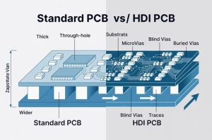
At its core, an HDI PCB is a type of printed circuit board that boasts a higher wiring density per unit area than conventional PCBs. This is achieved through several advanced manufacturing techniques that allow for finer lines, smaller spaces, and revolutionary interconnect structures.
The “High-Density Interconnect” refers to the ability to place more connections in a smaller area , leading to more compact and efficient circuit designs. Unlike traditional PCBs that rely on through-hole vias, HDI PCBs primarily utilize microvias—tiny holes drilled with lasers—which are essential for their compact design.
The innovation of HDI PCBs isn’t merely about making things smaller; it’s about optimizing functionality within constrained spaces.
By facilitating denser component placement and more efficient signal routing, HDI technology significantly improves electrical performance, reduces signal loss, and minimizes electromagnetic interference ( EMI). This makes them indispensable for any application where space is at a premium and performance is paramount, directly enabling the advanced capabilities we expect from modern electronic products.
3. Key Technologies Driving HDI Performance
The superior performance and miniaturization capabilities of HDI PCBs stem from a suite of specialized manufacturing technologies. These innovations collectively allow for the intricate designs and high reliability demanded by advanced electronics.
3.1. Microvias: The Tiny Connectors
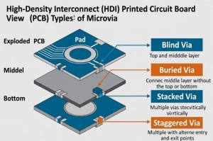
Microvias are arguably the most distinguishing feature of HDI PCBs. Unlike conventional through-hole vias, which typically have diameters of 0.2mm to 0.4mm and extend through multiple layers, microvias are much smaller, usually less than 0.15mm in diameter. They are blind (connecting an outer layer to an inner layer) or buried (connecting two inner layers) and are typically formed using laser drilling technology. This precision drilling allows for extremely fine pitches and greatly increases routing density. Microvias can be:
- Blind Vias:Connect an outer layer to one or more inner layers but do not pass all the way through the board.
- Buried Vias:Connect two or more inner layers and are completely contained within the PCB, invisible from the surface.
- Stacked Vias:Microvias directly stacked on top of each other, allowing for connections between many layers in a small footprint.
- Staggered Vias:Microvias placed adjacent to each other on different layers, offering greater flexibility in routing.
The choice between these types depends on the complexity and layer count of the board, significantly impacting overall design density and signal integrity.
3.2. Sequential Lamination and Build-Up Process
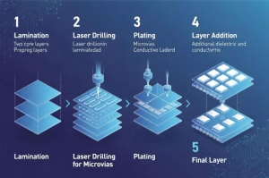
Standard PCBs are typically manufactured by laminating all layers simultaneously. HDI PCBs, however, often employ a sequential build-up (SBU) process. This involves adding layers one by one, with laser drilling and metallization steps performed after each new layer or set of layers is added.
This allows for the creation of complex stacked and staggered microvias that would be impossible with traditional methods. The sequential lamination process enables the creation of highly complex multi-layer boards with very thin dielectric layers, further contributing to miniaturization and improved electrical performance.
3.3. Fine Line Technology
HDI PCBs feature significantly finer lines and spaces compared to conventional PCBs. While standard PCBs might have trace widths and spaces of 0.12 5mm (5 mils) or more, HDI boards push these limits down to 0.075mm (3 mils) or even 0.05mm (2 mils). This fine line technology is critical for accommodating the increased density of components and interconnections, allowing more traces to be routed within a given area. Achieving such precision requires advanced etching processes and highly controlled manufacturing environments to prevent defects and ensure reliable connectivity.
3.4. Advanced Materials
The materials used in HDI PCBs are also crucial. They often incorporate thinner prepreg and core materials, and sometimes use specialized low-loss dielectric materials to optimize high-frequency performance and signal integrity. These materials must maintain excellent electrical properties and mechanical stability despite their reduced thickness, a critical factor for high-performance electronic products.
4. Unpacking the Benefits of HDI PCBs
The integration of micro-technology and advanced manufacturing processes in HDI PCBs translates into a multitude of benefits that are pivotal for modern electronics.
4.1. Extreme Miniaturization
This is perhaps the most obvious benefit. By using microvias, finer lines, and denser component placement, HDI PCBs dramatically reduce the overall size and weight of electronic devices. This allows for sleeker designs, more ergonomic products, and increased portability, essential for everything from consumer gadgets to compact medical equipment. A smaller PCB means a smaller final product, which is a major selling point in competitive markets.
4.2. Enhanced Electrical Performance and Signal Integrity
The shorter trace lengths and reduced via stubs inherent in HDI designs lead to superior electrical characteristics. Shorter signal paths mean less signal attenuation, reduced impedance mismatch, and lower parasitic capacitance and inductance. This translates into cleaner signals, higher operating frequencies, and improved overall performance, which is critical for high-speed digital circuits and RF applications.
4.3. Improved Reliability
With fewer through-hole vias, the mechanical stress on solder joints can be reduced. Additionally, the controlled manufacturing processes and advanced materials used in HDI PCBs contribute to increased robustness and longevity. The compact design can also help manage thermal dissipation more effectively in certain configurations, further enhancing device reliability over time.
4.4. Cost-Effectiveness (Long Term)
While the initial manufacturing cost per board might be higher than a conventional PCB, HDI technology often proves more cost-effective in the long run. By allowing for fewer layers to achieve the same routing density, or by enabling the use of smaller PCBs for the same functionality, it can reduce overall material usage and assembly costs. Moreover, the ability to integrate more features onto a single, compact board can simplify final product assembly and improve yield, ultimately leading to a lower total system cost.
4.5. Design Flexibility
The ability to place components closer together and route signals with greater freedom opens up new possibilities for designers. HDI technology allows for more complex circuit architectures and the integration of diverse functionalities onto a single board, which is crucial for multi-functional devices.
Here’s a comparison highlighting key differences:
| Feature | Standard PCB | HDI PCB |
| Wiring Density | Lower | Significantly Higher |
| Via Type | Primarily Through-Hole | Microvias (Blind, Buried, Stacked, Staggered) |
| Via Diameter | 0.2mm – 0.4mm (approx.) | < 0.15mm (approx.) |
| Trace Width/Space | 0.125mm (5 mil) or more | 0.075mm (3 mil) or less |
| Layer Count for Density | Higher for complex designs | Lower for comparable density |
| Signal Integrity | Good, but can suffer at high speeds | Excellent, especially at high speeds |
| Miniaturization | Limited | Enables extreme miniaturization |
| Manufacturing Process | Simultaneous Lamination | Sequential Build-Up ( SBU)common |
| Typical Applications | Basic consumer electronics, power supplies | Smartphones, wearables, medical, aerospace |
5. Where HDI PCBs Shine: Key Applications
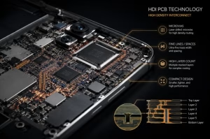
The unique advantages of HDI PCBs make them indispensable across a wide spectrum of industries, powering the most innovative and demanding electronic products.
5.1. Consumer Electronics
- Smartphones and Tablets :These devices are the quintessential examples of HDI PCB application. The need to pack powerful processors, high-resolution cameras, multiple sensors, and long-lasting batteries into ultra-thin form factors is entirely dependent on HDI technology.
- Wearable Devices:Smartwatches, fitness trackers, and AR/VR headsets require extremely compact and lightweight electronics that can conform to ergonomic designs. HDI PCBs are critical for enabling their small size and complex functionality.
- Laptops and Ultrabooks:To achieve their thin profiles and high performance, modern laptops extensively use HDI boards for their main logic boards and peripheral components.
5.2. Medical Devices
The medical industry heavily relies on HDI for precision and reliability. Applications include:
- Implantable Devices:Pacemakers, neurostimulators, and cochlear implants demand minute electronics with faultless performance and biocompatibility, often built on HDI.
- Diagnostic Imaging:Portable ultrasound machines, MRI components, and other diagnostic tools benefit from the high signal integrity and compact nature of HDI PCBs.
- Surgical Tools:Minimally invasive surgical instruments incorporate HDI to integrate advanced sensors and controls into tiny probes.
5.3. Automotive Electronics
As cars become more sophisticated, incorporating advanced driver-assistance systems (ADAS), infotainment, and engine management units, HDI PCBs are increasingly vital. They can withstand harsh automotive environments while supporting complex digital systems for features like autonomous driving, GPS, and advanced safety systems.
5.4. Aerospace and Defense
In aerospace, weight and space are critical. HDI PCBs are used in avionics, radar systems, and satellite technology where high performance, extreme reliability, and compact size are non-negotiable. Their ability to handle high -frequency signals is also a major asset in these demanding environments.
5.5. Industrial and IoT Devices
From smart factory sensors to advanced robotics and industrial control systems, HDI PCBs facilitate the integration of complex logic and connectivity into smaller, more robust packages, driving the ongoing revolution of the Internet of Things (IoT).
To see how these advantages can be applied to your specific project, you can view our full range of HDI PCB capabilities.
6. Manufacturing Complexities and Future Outlook
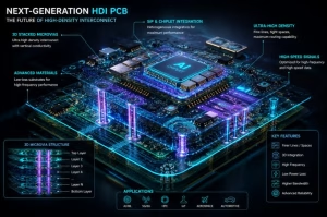
While offering immense benefits, the fabrication of HDI PCBs presents significant manufacturing challenges. The precision required for laser drilling microvias, the sequential lamination process, and the handling of ultra-fine lines demand specialized equipment, highly skilled technicians, and stringent quality control.
This complexity often translates into higher initial manufacturing costs and longer lead times compared to standard PCBs. However, advancements in automation, materials science, and laser technology are continuously improving efficiency and reducing costs.
The future of HDI PCBs looks incredibly promising. As the demand for even smaller , more powerful, and smarter devices continues to grow, HDI technology will evolve further. We can expect:
- Even Finer Features:Continued reduction in microvia sizes, trace widths, and spaces.
- Increased Layer Counts and Stacking:More sophisticated stacked and staggered via structures for ultra-high density.
- Integration of New Materials:Development of novel dielectric materials for higher frequencies and improved thermal management.
- 3D Integration:Closer integration with packaging technologies like System-in-Package (SiP) and 3D IC stacking, blurring the lines between PCB and semiconductor manufacturing.
HDI PCBs are not just a current trend but a foundational technology that will continue to shape the electronic landscape for decades to come, enabling innovations we can only begin to imagine.
7. FAQ
- Question1:What is the main difference between HDI and standard PCBs?
Answer: The primary difference lies in wiring density, achieved through features like microvias (laser-drilled, small vias) and finer line technology in HDI PCBs, which are largely absent in standard PCBs that rely on larger, mechanical through-hole vias. This enables HDI to achieve much greater miniaturization and performance. - Question2:Are HDI PCBs always more expensive?
Answer : The initial fabrication cost per board for HDI PCBs is typically higher due to specialized equipment and processes. However, their ability to reduce board size, lower layer count for complex designs, and improve overall system reliability can lead to significant cost savings in the long term, making them more cost-effective for advanced applications. - Question3:What are microvias?
Answer: Microvias are tiny, laser-drilled holes in an HDI PCB, typically less than 0.15mm in diameter. They connect different layers of the PCB, but unlike traditional through-hole vias, they are often blind (connecting an outer layer to an inner) or buried (connecting two inner layers), allowing for much denser routing and component placement. - Question4:Which industries benefit most from HDI PCBs?
Answer: Industries requiring extreme miniaturization, high performance, and robust reliability benefit most. These include consumer electronics (smartphones, wearables), medical devices (implants, diagnostic equipment), automotive (ADAS, infotainment), and aerospace/defense.
8. Summary
High-Density Interconnect (HDI) PCBs are a cornerstone of modern electronics, enabling the extreme miniaturization and high performance demanded by today’s devices.
Through advanced manufacturing techniques such as laser-drilled microvias (blind, buried, stacked, staggered), sequential lamination, and fine line technology, HDI boards achieve unparalleled wiring density. These innovations translate into significant benefits including smaller form factors, enhanced electrical performance, superior signal integrity, improved reliability, and long-term cost-effectiveness.
From powering the latest smartphones and wearables to critical medical implants and advanced automotive systems, HDI PCBs are indispensable, continuously evolving to meet the escalating demands of a connected and compact world. Their ongoing development promises to unlock even greater possibilities for future electronic innovations.
Ready to start your HDI PCB project? Get a quote today and let our experts help turn your ideas into reality.
9. Key Takeaways
- Miniaturization Driver:HDI PCBs are crucial for reducing the size and weight of electronic products without sacrificing performance.
- Microvias are Key:Tiny, laser-drilled microvias (blind, buried , stacked) are the hallmark of HDI, enabling high-density routing.
- Performance Boost:Expect improved signal integrity, higher operating frequencies, and reduced signal loss with HDI technology.
- Broad Applications :Essential for smartphones, wearables, medical devices, automotive, and aerospace electronics.
- Advanced Manufacturing:Utilizes sequential build-up and fine line technology, demanding specialized processes.
- Future-Proof ing:Continues to evolve, promising even greater density and integration for future electronic innovations.
As part of the same trusted team, we are excited to introduce our brand: OrinewPCB for faster, high-quality One-Stop PCB assembly services.
Related Posts
ORINEWPCB · PROJECT SUPPORT
Contact Us
Discuss your PCB assembly project with our team.
FREE QUOTE
Plan your turnkey PCBA build.
Share your quantity and requirements. Add Gerber files and a BOM when ready.
Files are optional for an initial discussion. Include any assembly, sourcing or testing requirements in your message.