Flexible Printed Circuit Boards: Everything You Should Know

Table of Content
With the electronics industry trending towards lighter, smaller, and more highly integrated and reliable products, flexible PCBs have broken the form limitations of traditional rigid boards. Their ability to bend and fold offers revolutionary design freedom and performance breakthroughs for fields like wearables, medical devices, aerospace, automotive, and consumer electronics.
However, designing and manufacturing flex PCBs is far more complex than rigid boards. It involves challenges in materials, mechanics, electrical engineering, and processing. Engineers often need to balance functional requirements with manufacturing standards. Every step, from precision profiling and copper layer selection to the use of stiffeners, requires careful consideration.
1. What is a Flexible PCB?
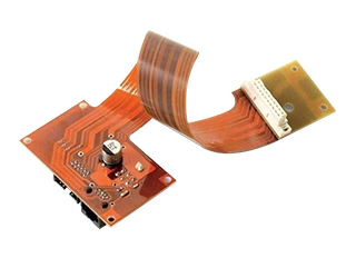
A flexible printed circuit board is a circuit board built on a flexible base material. Its key feature is the ability to bend, fold, or twist during installation or use without causing electrical failure. The fundamental difference from traditional rigid PCBs (which use materials like FR-4) is the substrate: flex PCBs use flexible films like Polyimide (PI) or Polyester (PET).
2. Understanding Flex PCB Bending Performance
Bending performance is the core difference between flexible and rigid PCBs and a critical design consideration.
2.1 Static vs. Dynamic Bending
- Static Bending (Installation Bend):The FPC is bent into a specific shape once during product assembly and then fixed. For example, in a phone hinge or camera module.
- Dynamic Bending (Repeated Bending):The product requires repeated bending throughout its lifespan. Examples include cables in flip-phone hinges or robotic arms.
Dynamic bending places much higher demands on material fatigue life, copper type, and structural design.
2.2 Minimum Bend Radius
This is one of the most critical design parameters. It’s the smallest radius the board can be bent without mechanical damage or electrical failure.
(1)Calculation Rules of Thumb:
Single-Sided: Minimum Bend Radius ≥ 6 × Total Board Thickness
Double-Sided/Multi-Layer: Minimum Bend Radius ≥ 12 × Total Board Thickness
(2)Influencing Factors:
Material Thickness: Thicker substrates, copper, and coverlay require a larger bend radius.
(3)Copper Type:
Rolled-Annealed (RA) Copper: Has elongated grains, offering excellent flex life. It’s the top choice for dynamic bending but costs more.
Electrodeposited (ED) Copper: Has a vertical grain structure, offering less flexibility. Better for static bending or simple installation.
Trace Direction: For bending, traces should run perpendicular to the bend axis to minimize stress. Traces parallel to the axis are more likely to crack on the outer curve.
Stack-up: In bending areas, aim to keep the copper layers near the neutral axis of the stack-up to reduce tensile and compressive stress. This often requires a “symmetric stack-up.”
2.3 Golden Rules for Bending Area Design
- Avoid placing vias, pads, or components in the bending area.
- Route traces gradually into/out of the bend area. Avoid sharp 90° turns; use arcs or 45° angles.
- Use a cross-hatched or “hatched” copper pattern instead of solid copper in bending areas to improve flexibility and prevent wrinkling.
- For dynamic bending, RA copper is mandatory.
3. Understanding Flex PCB Materials
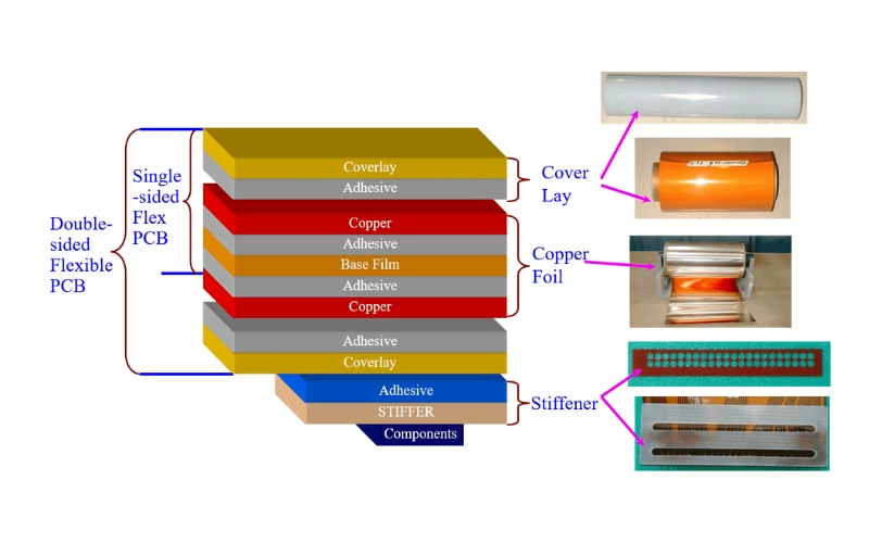
Materials are the foundation of flex PCB performance, reliability, and cost.
3.1 Substrate
- Polyimide (PI) (e.g., DuPont Kapton):
Pros: Extremely high thermal stability (-269°C to +400°C), excellent mechanical properties, good chemical resistance, high insulation, UL94 V-0 flame retardant. It’s the dominant choice for high-performance flex PCBs.
Cons: Absorbs some moisture, higher cost.
- Polyester (PET) (e.g., Mylar):
Pros: Low cost, good moisture resistance, acceptable electrical properties.
Cons: Poor heat resistance (typically <105°C), difficult for soldering, less dimensionally stable than PI. Used in low-end, non-soldered consumer products (e.g., keyboard membrane circuits).
- Modified Polyimide, Liquid Crystal Polymer (LCP):Used for ultra-high frequency (mmWave) applications due to very low and stable dielectric constant and loss factor, and very low moisture absorption.
3.2 Conductor Layer (Copper Foil)
Electrodeposited (ED) Copper: Formed by electroplating. Lower cost, rough surface (good for adhesion), but low ductility. Suitable for static applications.
Rolled-Annealed (RA) Copper: Formed by mechanical rolling. Elongated grain structure provides excellent ductility and flex life. It’s essential for dynamic bending. The surface is smoother, sometimes requiring special treatment for adhesion.
Copper Weight: Common choices are 1/2 oz (18µm), 1 oz (35µm), and 2 oz (70µm). Thinner copper (e.g., 1/3 oz) is more flexible but has lower current capacity and requires more precise etching.
3.3 Coverlay
Function: Replaces the solder mask used on rigid PCBs, providing insulation and protection.
Material: Typically a polyimide film (e.g., 12.5µm, 25µm thick) coated with a thermoset adhesive (acrylic or epoxy).
Process: Openings are pre-cut using lasers or dies based on Gerber files. The coverlay is then laminated onto the circuit using heat and pressure. Registration accuracy is critical.
3.4 Adhesive
Acrylic: Good flexibility, suitable for dynamic bending, but lower heat resistance (~125°C).
Epoxy: High bond strength, good heat resistance (~150°C), but less flexible.
Adhesiveless: Copper is directly bonded to PI using coating or sputtering. This eliminates the adhesive layer, resulting in a thinner product, higher heat resistance (>200°C), better dimensional stability, and superior flexibility. It’s the trend for high-end applications.
3.5 Stiffener
Polyimide (PI) Stiffener: Matches the thermal expansion of the base material. Often used behind gold fingers to reinforce them for connector insertion.
FR-4 Stiffener: Lower cost, used in areas needing basic rigid support.
Stainless Steel (SUS) Stiffener: Very high strength and flatness, precise thickness. Ideal for SMT assembly areas, especially for fine-pitch components. Be mindful of its conductivity and magnetic properties.
4. Understanding Flex PCB Layout and Routing
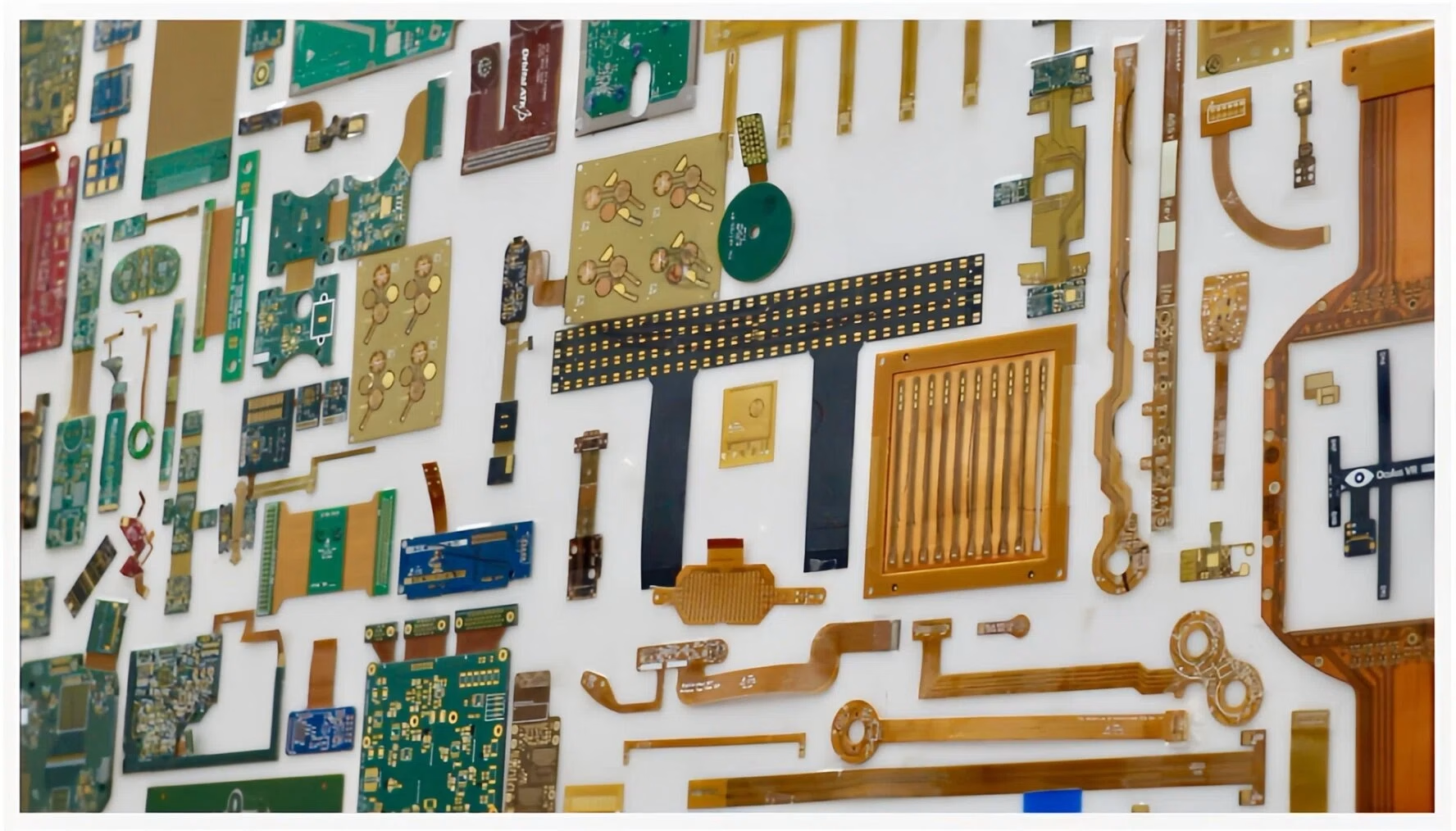
Layout and routing are central to flex PCB design, directly impacting electrical performance, manufacturability, and reliability.
4.1 General Design Guidelines
(1)Profile and Drilling:
Distance from through-holes/pads to board edge ≥ 0.5mm. Use mouse bites (U-shaped slots) if this is not possible.
Distance from via edge to solder mask opening edge ≥ 0.2mm to prevent copper exposure.
Avoid vias-in-pad, as FPCs can’t be resin-plugged, leading to solder wicking.
(2)Copper and Pad Design:
Large solid copper areas: Can trap gas during lamination, causing oxidation and blistering. Use hatched copper or add openings in the coverlay for outgassing.
Isolated pads are prone to peeling: Use teardrops or anchor pads to connect them securely to adjacent copper or traces. On double-sided boards, stagger pads on opposite sides.
Connector pads: Use Solder Mask Defined (SMD) pads, where the coverlay opening is smaller than the copper pad. This allows the coverlay to hold down the pad edges, providing mechanical anchoring.
Avoid large areas of exposed copper without coverlay to prevent wrinkling and oxidation.
(3)Coverlay Opening Rules:
Gap between a pad and adjacent trace ≥ 0.2mm.
Gap between pads ≥ 0.5mm. Otherwise, use a “bridge” of coverlay between them.
(4)Gold Fingers and Soldering:
Gold Fingers: The trace connecting to the finger should be stepped back (necked down) by about 0.2mm from the finger’s base. This prevents micro-shorts from carbonization during laser cutting.
Coverlay at Finger Root: The coverlay should extend over the base of the finger copper by at least 0.3mm to provide stress relief and prevent the finger from peeling off.
Solder Mask Opening for Fingers: The coverlay opening must be larger than the finger copper to ensure the connector contact presses fully on the finger.
(5)Vias and Test Points:
Vias in bend areas are prone to cracking and are usually covered by the coverlay.
Test points should be designed as bare copper pads with a coverlay opening, not marked simply as vias.
4.2 Routing Specifics
Trace Angles: Use 45° angles or curves, avoid 90° corners.
Trace Routing: In bending areas, distribute traces evenly instead of running many parallel traces close together. Use fan-out routing where needed.
Power/Ground Traces: Make them wider than signal traces. Use hatched or cross-hatched patterns for ground planes in flexible areas to maintain flexibility.
Impedance Control: High-frequency signal traces require impedance calculation. Input the flex material’s dielectric constant (~3.4 for PI) and dielectric thickness accurately into simulation software. Due to the coverlay and adhesive, simulation results should be verified through prototyping and TDR (Time Domain Reflectometry) testing.
5. Choosing the Right Flex PCB Stack-up
The stack-up defines the circuit’s physical and electrical characteristics. Choices involve trade-offs between flexibility, thickness, cost, impedance, and heat dissipation.
5.1 Common Stack-up Types
- Single-Sided (1-Layer):Structure: Coverlay / Copper / Substrate. Simplest, most flexible, lowest cost.
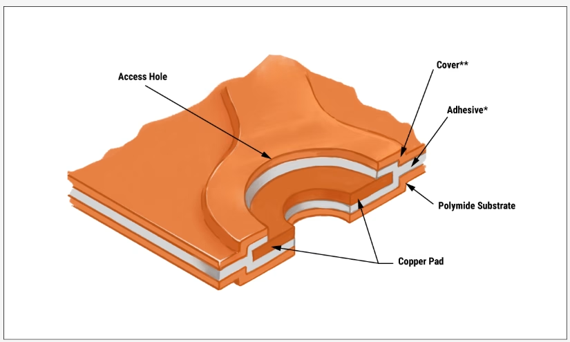
- Double-Sided (2-Layer):Structure: Coverlay / Copper / Substrate / Copper / Coverlay. Interconnection via plated through-holes. The most common general-purpose structure.
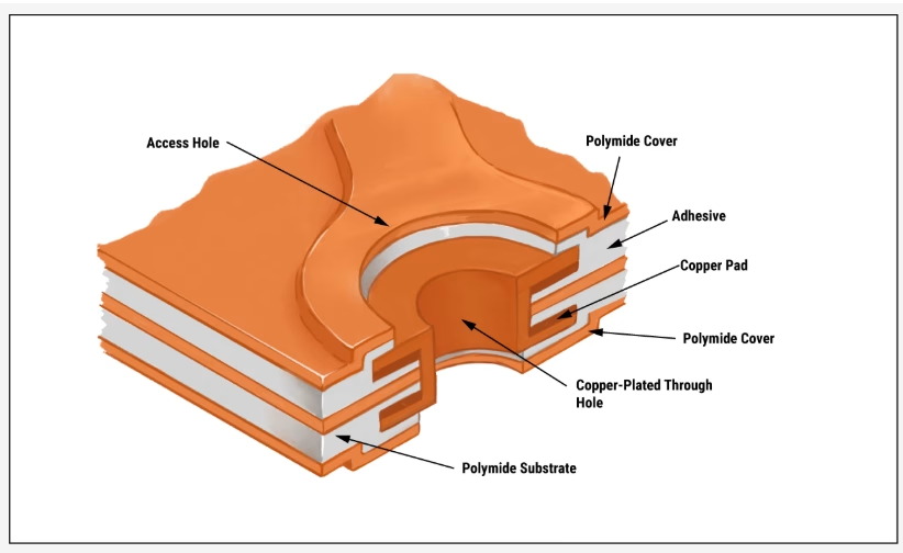
- Multi-Layer Flex:Several double-sided structures laminated together with bonding sheets (prepreg). High complexity, high cost, reduced flexibility.
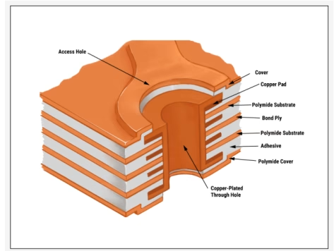
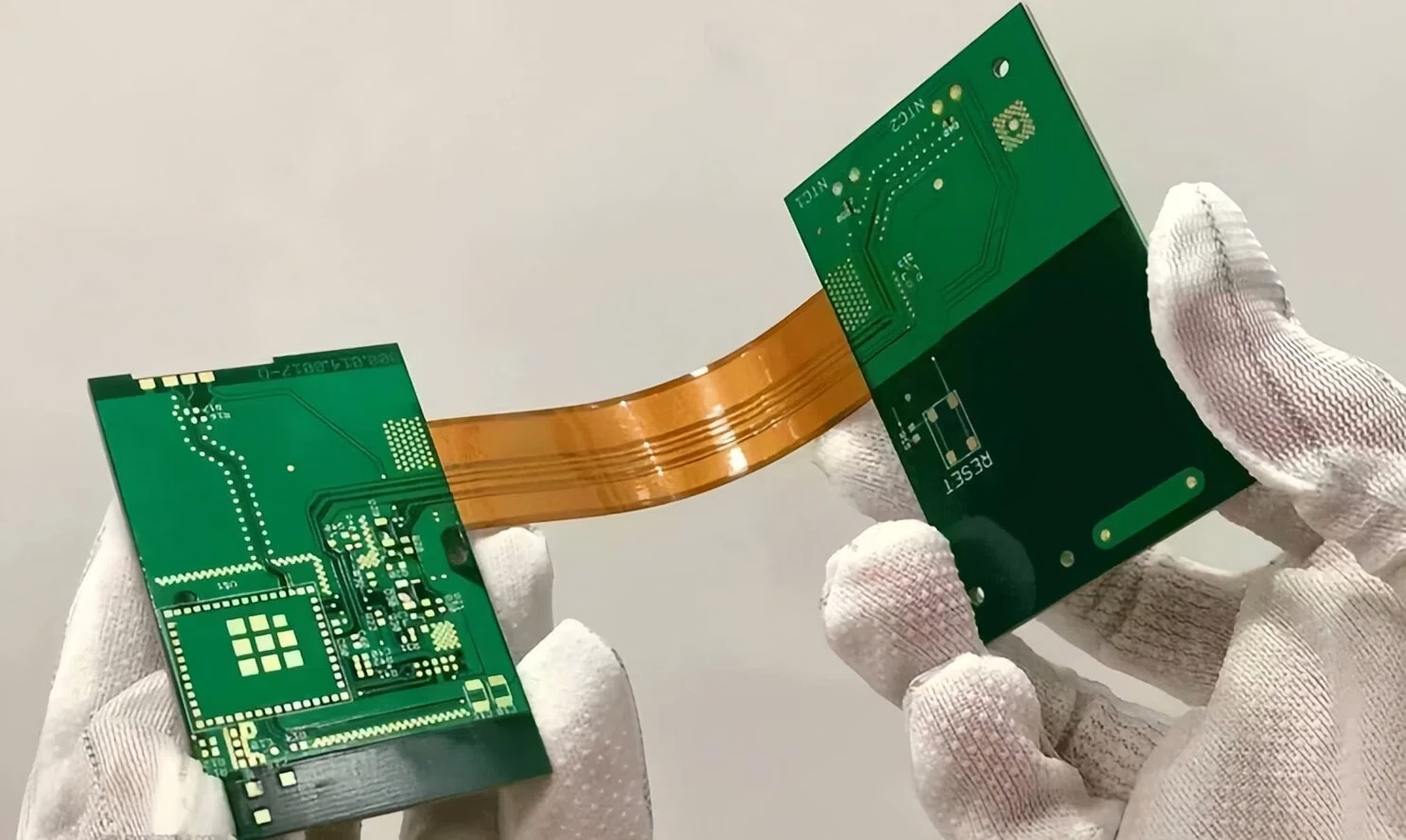
- Rigid-Flex:Rigid (FR-4) and flexible (PI) sections laminated in one process. Most complex design, but offers optimal 3D assembly and reliability.
5.2 Design Considerations
Symmetry: For double-sided or multi-layer boards, design a symmetric stack-up (e.g., symmetric copper and coverlay thicknesses) to balance stress and prevent warping during bending.
Total Thickness: Know the final thickness requirements, especially for areas that need to fit into connectors (Total thickness = Substrate + Copper + Coverlay + Stiffener).
Adhesiveless vs. Adhesive-Based: For high-density, high-frequency, or high-temperature applications, prioritize adhesiveless materials.
Consult Your Fabricator: Before finalizing the stack-up, discuss it with your PCB manufacturer. Use their standard material library and process capabilities for the most cost-effective and manufacturable solution.
6. Standards for Flex PCB Design, Manufacturing, and Testing
6.1 Main Industry Standards
IPC Standards:
IPC-6013: “Qualification and Performance Specification for Flexible/Rigid-Flexible Printed Boards” – The core standard for manufacturing and acceptance, defining classes (Class 1, 2, 3) and performance requirements.
IPC-2223: “Sectional Design Standard for Flexible Printed Boards” – The authoritative guide for flex PCB design, covering materials, layout, electrical, and mechanical aspects.
IPC-FC-234: “Guidelines for Pressure-Sensitive Adhesives for Assembly of Flexible Circuits”.
IPC/JPCA-6202: “Performance Guide for Single and Double-Sided Flexible Printed Wiring Cables”.
UL Standards (Underwriters Laboratories): UL 94 (Flammability), UL 746E (Polymeric Material Evaluation) – Relevant for product safety certification.
Military and Aerospace Standards: e.g., MIL-P-50884 (largely superseded but still referenced), with extremely high reliability requirements.
6.2 Key Manufacturing Process Steps
DFM (Design for Manufacturability) Check: Manufacturer checks Gerber, drill files against their process capabilities.
Material Cutting and Cleaning.
Pattern Transfer: Dry film or liquid resist is applied, exposed, and developed.
Etching: Unwanted copper is etched away.
Drilling: Mechanical or laser drilling for vias. Laser drilling enables microvias (<100µm).
Plating: Electroless copper + electrolytic copper plating to create conductive vias.
Coverlay Lamination: Pre-cut coverlay is laminated onto the circuit using heat and pressure.
Surface Finish: Pads are finished with ENIG, ENEPIG, immersion tin, or OSP. Gold fingers typically get electroplated hard gold for durability.
Profiling: Final shape cut using laser, die punching, or CNC routing. Laser cutting offers high precision for prototypes and complex shapes.
Electrical Test (E-Test): Flying probe or fixture test to verify circuit continuity.
Final Inspection and Packaging: Visual inspection (AOI), dimensional check. Flex PCBs require special antistatic, crush-resistant packaging.
7. Comparison: Rigid PCB vs. Flexible PCB vs. Rigid-Flex PCB
| Feature | Rigid PCB | Flexible PCB | Rigid-Flex PCB |
| Base Material | FR-4, Metal Core, Ceramic | Polyimide (PI), Polyester (PET) | Rigid area: FR-4; Flex area: PI |
| Core Feature | Fixed shape, structurally rigid | Can bend, fold, twist | Combines rigid support and flexible interconnection |
| Weight/Thickness | Heavier, thicker | Very light, very thin | Lighter than all-rigid, more robust than all-flex |
| Design Freedom | 2D plane | High, adapts to complex 3D space | Very high, optimal space use and reliability |
| Reliability | High, but connectors are failure points | High, reduces connectors and solder joints | Highest, monolithic construction eliminates board-to-board connectors |
| Vibration Resistance | Moderate | Excellent | Excellent |
| Heat Dissipation | Depends on material (Metal Core best) | Moderate (PI is not a good thermal conductor) | Can be optimized in rigid areas |
| Manufacturing Complexity | Low | Medium to High | Highest |
| Cost | Lowest | Higher (Materials + Process) | Highest (Design + Materials + Process) |
| Typical Application | Computer motherboard, appliance control board | Phone cables, camera module, wearables | Aerospace electronics, high-end medical (endoscopes), military equipment |
8. Applications of Flexible PCBs
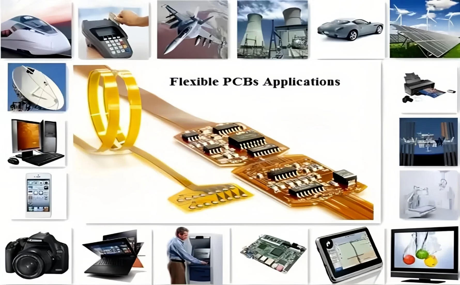
The unique advantages of flex PCBs make them the “hidden champion” in many cutting-edge fields.
(1)Consumer Electronics:
Smartphones/Foldables: Cables connecting mainboard to display, side keys, camera modules. Requires high dynamic flex life in hinges.
Laptops: Cables (LVDS/eDP) connecting mainboard to display through the hinge.
TWS Earbuds/Smartwatches: Connecting batteries, sensors, and mainboards in tiny spaces.
Drone Gimbal Cameras: Transmitting video signals while moving with the gimbal.
(2) Automotive Electronics:
LED Lighting: Flexible strips conforming to car body curves.
Sensors & Control Units: Parking sensors, camera modules, seat heating/pressure sensors, steering wheel controls. Must withstand heat, vibration, and chemicals.
Battery Management Systems (BMS): Sampling harnesses inside EV battery packs, requiring thinness, light weight, and safety.
(3)Medical Devices:
Wearable Monitors: ECG patches, Continuous Glucose Monitors (CGM). Require flexibility and biocompatibility.
Endoscopes/Catheters: Rigid-flex boards integrate sensors and LEDs at the tip, with the flex section transmitting signals through the shaft.
Ultrasound Probes: Interconnecting high-density transducer arrays.
(4)Industrial & Aerospace:
Industrial Robots: Dynamic signal transmission in robot arm joints.
Satellites/Spacecraft: Used for their light weight in connections between solar panels and sensors.
Military Equipment: Extremely high reliability requirements, often using rigid-flex designs.
(5)Emerging Fields:
Bio-based Flex PCBs: Using biodegradable or renewable materials (e.g., cellulose-based) for disposable medical devices or eco-friendly electronics. An area of ongoing research.
9. Flexible PCB FAQs
Static bending: Electrodeposited (ED) copper is usually sufficient and lower cost.
Dynamic bending (>10,000 cycles): You must use Rolled-Annealed (RA) copper. Also, follow bend radius rules strictly, avoid vias in the bend area, and use hatched copper.
The flexible substrate (e.g., 25µm PI) is much thinner and softer than rigid FR-4, providing less mechanical anchoring for pads.
Prevention:
Use Solder Mask Defined (SMD) pads, where the coverlay holds down the pad edges.
Add teardrops or anchor pads to connect isolated pads firmly to traces or copper areas.
On double-sided boards, stagger pads on opposite sides to avoid stress concentration.
Neck-down: The trace connecting to the finger should be stepped back (necked down) by 0.1-0.2mm from the finger base to prevent contamination from laser cutting.
Root Reinforcement: The coverlay must extend over the finger’s copper base by at least 0.3mm for support.
Backside Stiffener: Gold fingers usually need a PI stiffener on the back. The stiffener should extend beyond the finger contacts by at least 1.0mm for easy insertion and to prevent damage.
Surface Finish: Typically electroplated hard gold for wear resistance. Specify gold thickness (e.g., 0.5µm, 1.0µm).
Add tooling rails and fiducials for SMT assembly.
Use “break-away tabs” (mouse bites) to connect individual boards. Avoid placing tabs on edges with gold fingers.
Tab strength: Too small -> break during handling. Too large -> hard to depanelize. Typical width ~0.8mm, spacing 15-20mm. Very small boards may only need 2 tabs.
Very small circuits (<20x20mm) must be panelized to prevent them from being sucked away during handling.
Communicate your panelization needs to your fabricator; they can offer expert advice.
Yes, it’s more challenging than for rigid PCBs.
Reasons: Material non-uniformity (coverlay/adhesive thickness and Dk can vary slightly after lamination). Asymmetric stack-ups can affect reference planes.
Recommendation: Start your design using verified stack-up models and line width parameters from your manufacturer. It is essential to validate your design by fabricating impedance coupons and measuring them with a TDR (Time Domain Reflectometer), especially for high-speed signals.
Materials: Specialized flexible materials cost more and may not be kept in stock.
Process: More process steps (like coverlay cutting and lamination), and some steps are semi-automated or manual, making them less efficient.
Tighter Tolerances: Requirements for registration, cutting, etc., are often stricter.
Production Volume: Flex PCB batches are typically smaller, limiting economies of scale.
Advice: Plan ahead, communicate clearly with your flex board house, and using their standard processes can help optimize cost and lead time.
10. Conclusion
Flexible PCBs represent a new philosophy in circuitry—making the circuit conform to the product. Their successful application hinges on early planning and collaborative design. From the concept phase, you must comprehensively consider bending, spatial constraints, and environmental factors, and work closely with your manufacturer.
With the rapid growth of IoT, wearables, and automotive electronics, the future of flexible PCBs is bright. By mastering the core knowledge in this guide, you can leverage this powerful technology, overcome design barriers, and turn your most imaginative electronic products into reality.
Related Posts
ORINEWPCB · PROJECT SUPPORT
Contact Us
Discuss your PCB assembly project with our team.
FREE QUOTE
Plan your turnkey PCBA build.
Share your quantity and requirements. Add Gerber files and a BOM when ready.
Files are optional for an initial discussion. Include any assembly, sourcing or testing requirements in your message.