
Complete Guide to PCB Tinning

Printed Circuit Boards (PCBs) are the backbone of modern electronics, and their reliability is paramount. A crucial process in ensuring this reliability, particularly for long-term performance and robust connections, is PCB tinning. Essentially, PCB tinning involves coating the copper traces and pads of a PCB with a thin layer of tin or a tin alloy . This protective layer serves multiple vital functions, from enhancing solderability to preventing oxidation and corrosion.
While bare copper offers excellent conductivity, it is highly susceptible to oxidation when exposed to air. This oxidation forms a resistive layer that significantly impedes the soldering process, leading to weak or faulty connections. Tinning provides a barrier, ensuring that the copper remains pristine and ready for component assembly, whether through manual soldering or automated reflow processes. This comprehensive guide will delve into the various aspects of PCB tinning, exploring its methods, chemical compositions, practical applications, and troubleshooting common issues.
1. Introduction to PCB Tinning
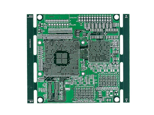
PCB tinning is to cover the untapped copper surface and create a solder mask with resins and paints. There is a better way to do this before copper oxidation and decomposition. It is called PCB tinning. PCB tinning is the process of coating copper traces with layers of tin, which will prevent it from any possible degradation, oxidation, or corrosion. The tin plating will also help mask copper traces while the circuit board itself is being etched.
Key Advantages of PCB Tinning:
- Enhanced Solderability:This is perhaps the most critical benefit. Tin has excellent wetting properties with solder, allowing molten solder to flow smoothly and create strong, reliable joints. By coating the copper, tinning prevents oxidation, which would otherwise make soldering difficult or impossible.
- Corrosion and Oxidation Resistance:Copper is highly reactive and readily oxidizes when exposed to air, moisture, and various environmental contaminants. The tin layer acts as a protective barrier, shielding the underlying copper from these elements, thereby significantly extending the shelf life and operational lifespan of the PCB.
- Improved Electrical Conductivity:While copper is highly conductive, the tin layer can maintain consistent surface conductivity over time by preventing the formation of resistive oxide layers, ensuring stable electrical performance.
- Uniform Surface Finish:Tinning provides a smooth, uniform surface finish, which is beneficial for automated component placement (pick-and-place machines) and ensuring consistent solder paste application.
- Cost-Effectiveness (in certain applications):Compared to some other surface finishes like gold plating, tinning can be a more economical choice while still providing excellent performance characteristics for many standard applications.
- Environmentally Friendly Options:Modern tinning processes often use lead-free tin, aligning with RoHS (Restriction of Hazardous Substances) directives and environmental sustainability goals.
2. Understanding PCB Tinning Methods
There are primarily two widespread methods for applying a tin coating to PCBs: electroplating (electrolytic tin plating) and electroless tin plating (immersion tin plating). Each method has its unique characteristics, advantages, and suitable applications.
2.1. Electroplating (Electrolytic Tin Plating)
Electrolytic tin plating, also known as tin electroplating or tin plating, is an electrochemical process where a direct current (DC) is used to deposit a layer of tin onto the copper surface of the PCB. The PCB acts as the cathode, while a tin anode or an inert anode is used in an electrolyte bath containing tin ions.
(1)Process Overview
- Preparation:The PCB surface must be thoroughly cleaned to remove any oils, oxides, or contaminants that could interfere with the plating process.
- Immersion: The clean PCB is immersed in an electrolyte solution containing tin salts (e.g., stannous sulfate, stannous fluoroborate), acids (e.g., sulfuric acid, methane sulfonic acid), and various additives (bright eners, grain refiners).
- Current Application:A DC current is passed through the bath. The tin ions in the solution migrate towards the negatively charged PCB (cathode) and are reduced, depositing metallic tin onto the copper surfaces . Simultaneously, tin from the anode (if soluble) dissolves into the solution to replenish the tin ions.
- Rinsing & Drying:After plating, the PCB is thoroughly rinsed to remove any residual electrolyte and then dried.
(2)Characteristics
- Produces a relatively thick and durable tin layer (typically 5-15 micrometers).
- Can result in a bright, aesthetically pleasing finish due to brightener additives.
- Offers excellent solderability and corrosion resistance.
- Requires electrical contact to all areas to be plated, which can be a limitation for complex designs or inner layers.
- More common for outer layers and components lea
2.2. Electroless Tin Plating (Immersion Tin Plating)
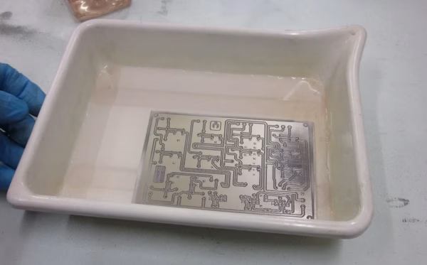
Electroless tin plating, often referred to simply as immersion tin, is a chemical deposition process that does not require an external electrical current. Instead, the tin deposition occurs through a displacement reaction between the copper surface and the tin ions in the plating solution.
(1)Process Overview
- Surface Preparation:The PCB undergoes a thorough cleaning process, followed by micro-etching to create an active copper surface.
- Immersion:The PCB is immersed in an acidic solution containing tin ions (typically stann ous chloride or stannous sulfate) and various complexing agents and stabilizers.
- Displacement Reaction:When the PCB is immersed, copper atoms on the surface donate electrons to the tin ions in the solution. The copper dissolves into the solution as copper ions, while the tin ions accept the electrons and deposit as a metallic tin layer onto the copper surface. This is a self-limiting reaction; as the tin layer forms, it eventually covers the copper, preventing further reaction.
- Rinsing & Drying:The PCB is then rinsed thoroughly and dried.
(2)Characteristics
- Produces a thinner tin layer (typically 0 .8-1.5 micrometers) compared to electroplating.
- Provides a uniform coating, even in complex geometries, since it doesn’t rely on current distribution.
- Ideal for fine-pitch components and BGA pads due to its flatness.
- Excellent shelf life for component assembly.
- Offers good solderability, though the thinner layer might have slightly less robust corrosion resistance than thick electrolytic tin over very long periods .
- The solution can become contaminated with dissolved copper, requiring careful maintenance or replacement.
2.3Comparison of Tinning Methods
| Feature | Electroplating (Electrolytic Tin ) | Electroless (Immersion Tin) |
| Process Type | Electrochemical (requires DC current) | Chemical Displacement (no external current) |
| Layer Thickness | Thicker (5-15 µm) | Thinner (0.8-1.5 µm) |
| Uniformity | Affected by current distribution, less uniform on complex shapes | Highly uniform, even on complex geometries |
| Application | Outer layers, component leads | Fine-pitch, BGA, internal layers (if applicable) |
| Solderability | Excellent, very robust | Excellent, good shelf life |
| Corrosion Resistance | Very High (due to thickness) | Good to High (can be affected by pinholes/porosity) |
| Cost | Can be higher due to equipment and power | Generally lower process cost per unit, but solution replacement cost |
3. The Chemistry Behind Tinning Solutions
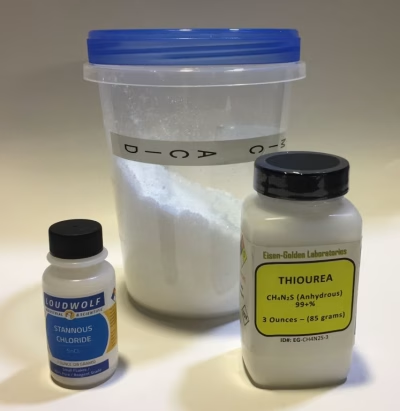
The effectiveness of both electrolytic and electroless tinning heavily relies on the precise composition of their respective plating solutions. These solutions are formulated with specific chemicals to achieve desired plating characteristics.
3.1Electrolytic Tin Plating Solutions
- Tin Source:Typically stannous sulfate (SnSO4) or stannous fluoroborate (Sn(BF4)2) provides the tin ions.
- Acid/Electrolyte:Sulfuric acid (H 2SO4) or methane sulfonic acid (MSA) is commonly used to maintain solution conductivity and prevent the hydrolysis of tin salts.
- Additives:
- Brighteners:Organic compounds that promote a finer grain structure, resulting in a shiny, bright tin deposit (e.g., aldehydes, ketones).
- Grain Refiners:Prevent the formation of large, uneven crystals, ensuring a smooth coating.
- Antioxidants:Prevent the oxidation of stannous ions (Sn2+) to stannic ions (Sn4+), which are not easily plated.
3.2Electroless Tin Plating Solutions
- Tin Source:Stannous chloride (SnCl2) or stannous sulfate (SnSO4) provides the Sn2+ ions for the displacement reaction.
- Complexing Agents:These agents keep the tin ions in solution and regulate their release for a controlled deposition. Common examples include thiourea, EDTA, or various organic acids.
- Acid/Stabilizer:Often contains an acid like hydrochloric acid (HCl) or sulfuric acid (H2SO4) to maintain the pH and prevent precipitation of tin compounds. Stabilizers are also crucial to prevent the premature decomposition of the bath and ensure a uniform, coherent tin layer.
- Accelerators:Sometimes used to speed up the deposition rate.
Maintaining the proper concentration of these components and controlling operating parameters like temperature and pH are critical for achieving a consistent and high-quality tin finish.
4. DIY PCB Tinning: A Hobbyist’s Guide
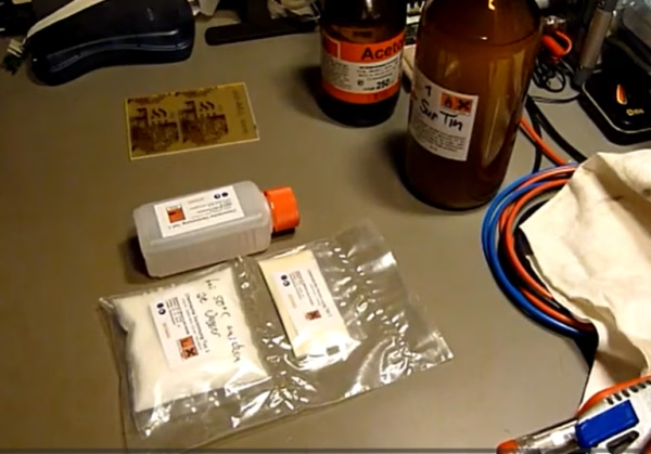
For hobbyists and small-scale prototyping, DIY PCB tinning offers a practical way to achieve professional -looking and functional boards without industrial equipment. Immersion tin plating is generally the preferred method for DIY due to its simpler setup compared to electroplating.
4.1 Materials Needed for DIY Immersion Tinning
- A clean PCB (etched and drilled).
- Commercial immersion tin plating solution (readily available from electronics suppliers).
- Non-metallic container (plastic or glass, resistant to mild acids).
- Distilled water for rinsing.
- Protective gloves, safety glasses, and adequate ventilation.
- Lint-free cloths or paper towels.
4.2DIY Process Steps
(1)PCB Preparation
- Thoroughly clean your PCB. Any remaining flux, grease, or oxides will prevent the tin from adhering. Use isopropyl alcohol or a dedicated PCB cleaner.
- A light scrubbing with a fine abrasive pad (e.g., Scotch-Brite) or fine steel wool (followed by thorough rinsing to remove debris) can help activate the copper surface, but be gentle not to damage traces.
- Rinse the PCB with distilled water immediately before tinning to remove any tap water impurities.
(2)Setting Up the Bath
- Pour the immersion tin solution into your non-metallic container. Ensure there’s enough solution to fully submerge the PCB.
- Work in a well-ventilated area and wear appropriate personal protective equipment (gloves, safety glasses).
(3)Immersion
- Carefully submerge the clean PCB into the tinning solution. You can agitate the solution gently or move the PCB around to ensure even coverage and dislodge any air bubbles.
- Follow the manufacturer’s recommended immersion time, usually a few minutes (e.g., 5-15 minutes). The copper surfaces will gradually change color to a silvery finish as tin deposits.
(4)Rinsing
Once the desired tin layer is formed, remove the PCB and rinse it thoroughly under running distilled water. This is crucial to remove all residual chemicals.
(5)Drying
Dry the PCB completely using a lint-free cloth, compressed air, or by allowing it to air dry.
4.3 Important DIY Safety Notes
- Always follow the safety instructions provided with your specific tinning solution.
- Wear chemical-resistant gloves and eye protection.
- Ensure good ventilation to avoid inhaling fumes.
- Dispose of spent solutions responsibly according to local regulations.
- Immersion tin solutions are typically mildly acidic; avoid contact with skin and eyes.
5. Common Challenges: Causes and Measures for Poor Tinning
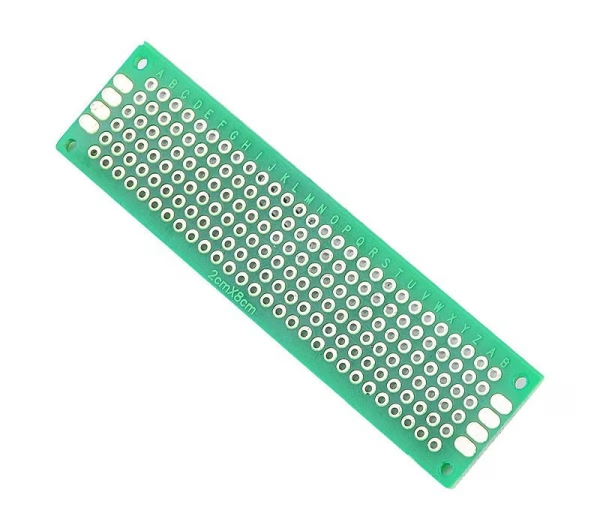
Despite its benefits, the tinning process can sometimes yield imperfect results, leading to issues like poor solderability, uneven coating, or delamination. Understanding the common causes is key to implementing effective corrective measures.
5.1 Causes of Poor Tinning
(1)Inadequate Surface Preparation: This is the most frequent culprit.
- Oxidation on Copper:If copper surfaces are not thoroughly cleaned or are exposed to air for too long before tinning, a thin oxide layer forms, preventing proper tin adhesion.
- Residual Contaminants:Oils, grease, fingerprints, flux residues , or etching residues left on the PCB surface act as barriers to tin deposition.
- Poor Micro-etching (Electroless):Insufficient or excessive micro-etching can lead to an inactive or rough copper surface, affecting uniformity.
(2)Issues with Plating Solution
- Depleted Chemicals:Over time, the active components (tin ions, brighteners, complexing agents) in the plating bath can be consumed or degrade.
- Contamination:Introduction of foreign ions (e.g., copper ions in electroless baths, iron, zinc), organic impurities, or particulates can disrupt the plating process.
- Incorrect Concentration:Too high or too low concentrations of key chemicals, including acids or additives.
- Temperature Fluctuations:Deviations from the optimal operating temperature can affect reaction rates and deposit quality.
(3)Process Parameter Errors (Especially Electroplating)
- Incorrect Current Density:Too low current density results in a thin, dull coating; too high can cause burning or rough deposits.
- Uneven Current Distribution:Poor racking or anode placement can lead to uneven plating thickness.
- Hydrogen Embrittlement:High current density in acidic baths can generate hydrogen gas, which can be absorbed by the base material, potentially causing embrittlement.
(4)Substrate Material Issues
- Inconsistent Copper Quality:Variations in the purity or surface characteristics of the copper foil can affect adhesion.
- Residual Laminate Resins:Smear or drilling residues in through-holes can prevent proper plating.
(5)Post-Treatment Issues
- Incomplete Rinsing:Residual plating solution can lead to corrosion or tin discoloration over time.
- Improper Drying:Leaving moisture on the surface can initiate oxidation.
5.2 Measures for Preventing and Correcting Poor Tinning
(1)Rigorous Cleaning Protocols
- Implement a multi -stage cleaning process (degreasing, rinsing, micro-etching, activating, final rinsing) tailored to the tinning method.
- Use high-quality cleaning agents and distilled/deionized water for rinsing.
- Ensure PCBs are processed immediately after cleaning to minimize re-oxidation.
(2)Bath Maintenance and Control
- Regularly analyze plating bath solutions to monitor and adjust concentrations of tin , acids, and additives.
- Filter solutions periodically to remove particulates and impurities.
- Control bath temperature strictly within specified limits.
- In electroless baths, monitor and replenish the tin source and adjust pH as copper contamination increases.
(3)Optimized Process Parameters
- For electroplating, use correct current density, ensure proper racking, and optimize anode-cathode spacing for uniform current distribution.
- Adhere strictly to recommended immersion times for electroless processes.
(4)Quality Control and Inspection
- Visually inspect PCBs before and after tinning for cleanliness and uniform coating.
- Use microscopy for detailed inspection of deposit quality and thickness.
- Conduct solderability tests on samples to verify process effectiveness.
(5)Material Selection
Ensure the base copper material meets specifications for purity and surface finish.
(6)Proper Storage
Store tinned PCBs in a dry, controlled environment, preferably in sealed, moisture-barrier packaging, especially for immersion tin which has a shorter shelf life than electrolytic tin.
6.FAQs
Electrolytic (electroplating) uses an external electric current to deposit a thicker tin layer, while electroless (immersion) plating uses a chemical displacement reaction to deposit a thinner, more uniform layer without current.
Tinning provides a protective barrier over the copper, preventing oxidation. Oxidized copper is difficult to solder to, while the tin surface readily wets with solder, forming strong, reliable joints.
The shelf life varies significantly. Electrolytic tin can last for months to over a year if stored properly. Immersion tin, being thinner, typically has a shorter shelf life, often 3-6 months , depending on storage conditions and environmental exposure.
Yes, DIY PCB tinning is feasible for hobbyists using commercial immersion tinning solutions. It requires careful surface preparation and adherence to safety guidelines.
Dullness or patchiness often results from inadequate surface cleaning , depleted plating bath chemicals (especially brighteners), incorrect bath temperature, or improper current density (in electroplating).
7.Summary
PCB tinning is an indispensable process in electronics manufacturing, vital for ensuring the long-term reliability and performance of printed circuit boards. By applying a protective layer of tin or a tin alloy onto copper traces and pads, tinning significantly enhances solderability, provides robust resistance against corrosion and oxidation, and improves electrical conductivity. The two primary methods, electrolytic and electroless tinning, each offer distinct advantages suitable for different applications, from thick, durable coatings for outer layers to uniform, flat finishes for fine-pitch components.
Successful tinning relies heavily on meticulous surface preparation, precise control over plating solution chemistry, and adherence to optimized process parameters. Understanding the causes of common defects, such as insufficient cleaning or contaminated baths, allows for effective troubleshooting and the implementation of corrective measures, ensuring high-quality and consistent results. For hobbyists, immersion tinning provides an accessible route to apply this critical surface finish, underscoring its broad utility across the electronics spectrum.








