
Application of Electromagnetic Compatibility(EMC) Design in PCB

In today’s highly electronic world, the number of electronic devices around us is growing exponentially. While these devices bring convenience, they also present a serious challenge: electromagnetic interference (EMI). Have you ever wondered why electronic devices must be turned off during airplane takeoff, or why mobile phone use is prohibited in certain hospital areas? The regulations behind these scenarios are closely related to a key technology: Electromagnetic Compatibility (EMC).
In practical engineering, over 70% of EMC issues can be traced back to the design stage of the printed circuit board (PCB). As the carrier for interconnecting electronic components, the layout, routing, and stack-up design of a PCB directly determine the final product’s EMC performance. This article will systematically explain the key EMC techniques in single/double-layer and multi-layer PCB design, starting from fundamental principles, providing engineers with a complete design guidance framework.
1.Definition of EMC

Electromagnetic Compatibility (EMC) is a critical performance metric that measures an electronic device’s ability to operate without faults in a shared electromagnetic environment (immunity) and not to become a source of electromagnetic interference for other devices (emission control). It is an essential requirement for modern electronic devices.
Its core encompasses two capabilities:
First, the device can operate stably in its intended electromagnetic environment without performance degradation or malfunction due to external interference (immunity).
Second, the device itself does not generate unacceptable electromagnetic interference for other systems (emission reduction).
These two aspects together form the foundation for the harmonious coexistence of electronic devices and the electromagnetic environment.
2.EMC Design for Single/Double-Layer PCBs
2.1 Component Placement Principles
Component placement is the starting point of PCB design. Proper placement can reduce the generation and propagation of EMI from the source.
Layout by functional grouping is the primary principle. Circuits of different types and characteristics should be physically isolated, forming clear functional partitions:
- Power Grouping:Circuits with different voltage levels should be placed separately. High-voltage, high-current power circuits must be isolated from low-voltage, small-signal circuits.
- Digital-Analog Separation:Digital and analog circuits must be strictly separated. Digital signals, with their sharp rising/falling edges, generate rich harmonic content and are major interference sources. Analog circuits are highly sensitive to minor noise and easily disturbed.
- Speed Separation:High-speed circuits (e.g., clock circuits, high-speed data buses) should be separated from low-speed circuits to prevent coupling interference.
- Power Separation:High-current drive circuits (e.g., motor drives, power switches) should be separated from small-signal processing circuits.

Centralized Connector Placement is another key principle. All external interface connectors should be placed on the same side of the PCB as much as possible. This effectively reduces the “antenna effect” of cables. When common-mode noise exists on the PCB, connected cables can become efficient radiating antennas. Concentrating all cables on one side can alter the radiation pattern and reduce overall radiation efficiency.
Optimized Layout of High-Speed Devices and I/O Drivers requires case-specific trade-offs:
- When there is no direct signal exchange between high-speed digital devices and connectors, place the high-speed devices away from connectors to reduce the likelihood of their noise radiating outward via cables.
- I/O drivers (e.g., serial transceivers, network PHY chips) must be placed close to their corresponding connectors. This ensures external signals are processed immediately upon entering the PCB, avoiding noise coupling during long-distance transmission.
- For high-speed devices that must communicate with connectors, use the shortest direct connection path, then surround them with medium/low-speed circuits as a buffer.
2.2 Ground and Power Trace Design

The “Split Ground” principle is an effective method for handling grounding in complex circuits. Its core idea is to establish multiple independent ground systems based on circuit characteristics, connected at a single point. Implementation includes:
- Digital Ground:Provides a clean reference for all digital circuits, especially focusing on grounding quality for high-speed digital sections.
- Analog Ground:Provides a pure reference environment for analog circuits, avoiding contamination from digital noise.
- Power Ground:Establishes a dedicated grounding path for high-current power circuits, preventing voltage drops on the ground trace from affecting sensitive circuits.
- Shield Ground:Provides dedicated grounding for metal enclosures, shields, etc.
After splitting, the independent ground systems should be connected at a single point near the power input, ensuring a unified reference potential for the entire system.
Power System Design needs to focus on loop control:
- Tight Coupling of Power and Ground Traces:Power and ground traces should be as wide and close together as possible, forming a low-inductance power supply loop. Loop inductance L is calculated as: L = μ₀μᵣA / l, where A is the loop area and l is the average perimeter. Reducing loop area directly lowers loop inductance.
- Avoid Overlapping Power Loops:Power supply loops for different sources should avoid spatial overlap to prevent interference via magnetic field coupling.
- Proper Use of Decoupling Capacitors:Place decoupling capacitors of appropriate value near the power pins of each IC to provide local energy storage for high-frequency switching currents. A typical configuration is: a 10μF electrolytic capacitor for low-frequency decoupling, a 0.1μF ceramic capacitor for mid-frequency decoupling, and a 100pF ceramic capacitor for high-frequency decoupling.
In double-layer boards, an interdigitated mesh power supply structure can optimize current distribution. By branching thinner traces perpendicularly from the main power trace, the overall impedance of the power distribution network is reduced, and multiple parallel paths are provided for return currents.
2.3 Signal Trace Design

Isolation of Incompatible Signal Traces is a fundamental routing principle. Incompatible traces include:
- High-frequency vs. low-frequency signal traces
- Digital vs. analog signal traces
- High-current vs. low-current signal traces
- Input vs. output signal traces
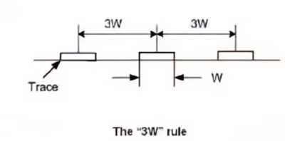
These traces should maintain sufficient distance and avoid long parallel runs. If routing on the same layer is necessary, the 3W rule is recommended: the center-to-center spacing between traces should be no less than three times the trace width.
Minimizing Signal Loop Area is the most effective means to reduce radiated emissions. According to electromagnetic radiation theory, the radiated power of a small loop antenna is proportional to the square of the loop area, current, and frequency: P_rad ∝ (I·A·f²)². In practical design:
- Each signal trace should have a clear, adjacent return path.
- High-speed signal traces should be routed on layers close to a ground plane.
- Avoid forming large loops with signal traces.
Impedance Matching is crucial for high-speed signal transmission. When the electrical length (delay corresponding to physical length) of a trace exceeds one-quarter of the signal rise time, transmission line effects must be considered, and impedance matching is required. Typical matching methods include:
- Source Series Termination:A series resistor at the driver output, with a value equal to the difference between the transmission line characteristic impedance and the driver output impedance.
- End Parallel Termination:A resistor in parallel at the receiver input to ground or power.
- Thevenin Termination:A voltage divider resistor network providing appropriate bias and matching.
High-Frequency Decoupling at I/O Ports can effectively suppress the ingress of external interference and radiation of internal interference. Appropriate high-frequency decoupling capacitors should be placed between the signal pins of each I/O connector and ground. The capacitor value should effectively filter expected high-frequency noise without affecting normal signal transmission.
3.EMC Design for Multi-Layer PCBs

3.1 Layer Stack-up Principles
The layer stack-up design of a multi-layer board is fundamental to its EMC performance. A proper stack-up provides inherent electromagnetic shielding and noise suppression capabilities.
Adjacent Power and Ground Plane Placement is the most important principle. Placing power and ground planes adjacent to each other enables:
- Distributed Decoupling Capacitance:The large copper planes form a natural parallel-plate capacitor. Capacitance C = ε₀εᵣA / d, where A is the overlap area and d is the dielectric thickness. This distributed capacitance provides a low-impedance return path for high-frequency noise.
- Electromagnetic Shielding:The ground plane can act as a shield for power plane noise, preventing it from radiating into space.
Signal Layers Adjacent to Reference Planes is another key principle. Each high-speed signal layer should be adjacent to a solid reference plane (ground or power plane). This allows for:
- Controlled characteristic impedance
- A clear, tightly coupled path for signal return currents
- Flux cancellation, reducing radiated emissions
Layer Isolation for Digital and Analog Circuits is easier to achieve in multi-layer boards. Ideally, digital and analog circuits should be placed on different signal layers, using independent power and ground planes. If sharing the same layer is necessary, ground plane splits and physical isolation zones should be used to reduce mutual interference.
Separate Layout for Clock and High-Frequency Circuits requires special attention. These circuits should be concentrated in a specific area of the PCB and kept as far away as possible from sensitive circuits and I/O ports. For particularly sensitive clock circuits, consider additional protection using local shields.
3.2 Two Key Spacing Principles
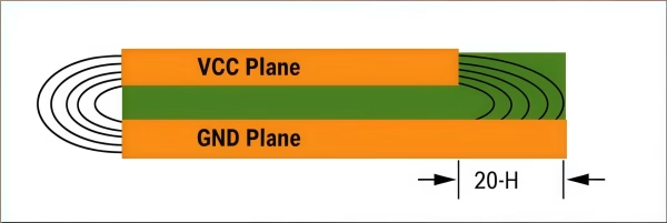
The 20-H Rule controls radiation from power plane edges. The power plane should be recessed inward from the edge of the adjacent ground plane by a distance of 20H (where H is the dielectric thickness between the two layers). This measure significantly reduces the intensity of edge field radiation. For a typical 1.6mm thick PCB, 20H is approximately 3mm.
The theory behind the 20-H rule: When power and ground plane edges are aligned, the electromagnetic field at the edge radiates into space. Recessing the power plane causes the edge field to close primarily between the two planes, greatly reducing radiation into space. Studies show radiation decreases significantly at 10H and by about 70% at 20H.
The 3W Rule is a fundamental geometric constraint in PCB design for controlling electromagnetic crosstalk between parallel traces. The rule states: To ensure coupling interference between adjacent signal traces is below the system’s acceptable threshold, the center-to-center spacing between two parallel traces should be no less than three times the width of a single trace (or equivalently, edge-to-edge spacing should be no less than twice the trace width).
More precise crosstalk control requires considering:
- Signal Edge Rate:Sharper edges (smaller rise time tr) contain more high-frequency components, widening the crosstalk spectrum and increasing coupled energy.
- Parallel Run Length:Crosstalk is a cumulative effect integrated over length; longer runs increase total coupling.
- Dielectric Properties:The dielectric constant directly affects the distributed capacitance and mutual inductance between traces, core determinants of coupling strength.
- Reference Plane Integrity:A solid reference plane provides a clear, low-impedance return path for signals. Discontinuities force return currents to take longer paths, increasing loop area and significantly altering/exacerbating electromagnetic coupling.
For differential signals, besides the 3W rule, consistent intra-pair spacing must be maintained for good common-mode rejection ratio.
3.3 Ground and Power Plane Design

The Concept of Distributed Parameters is crucial in high-frequency design. Above a certain frequency, conductors can no longer be considered ideal zero-impedance connections; their distributed parameters must be considered. For a typical PCB trace:
- Resistive Characteristic:Dominant at DC and low frequencies.
- Inductive Characteristic:A 25mm trace has approximately 15-20nH inductance, presenting about 10-12Ω impedance at 100MHz.
- Capacitive Characteristic:Distributed capacitance forms between the trace and reference plane, about 1-2pF/cm.
Power Plane-Ground Plane Structures offer significant advantages over trace-based power distribution:
- Extremely Low Power Supply Impedance:Plane structures can achieve characteristic impedance below 1Ω, much lower than trace pairs.
- Minimized Power Delivery Loops:Components connect directly to power/ground planes via vias, minimizing the power loop area.
- Distributed Decoupling Capacitance:The natural capacitance between power and ground planes provides high-frequency decoupling.
- Automatic Return Paths:Signal return currents automatically flow on the ground plane directly beneath the signal trace, forming the smallest signal loop.
In practical design, note: - Maintain the integrity of power and ground planes, avoiding excessive splits.
- Critical signal traces should not cross ground plane split gaps.
- Appropriately recess power plane edges to reduce edge radiation.
- Place decoupling capacitors rationally to cover broad frequency band impedance requirements.
3.4 Clock Circuit Design
The clock circuit is the heart of a digital system and often the primary interference source. Its design requires special care.
Impedance Control is foundational for clock circuit design. Clock signals are typically treated as transmission lines, requiring strict control of their characteristic impedance. Characteristic impedance for microstrip and stripline can be estimated:
- For Microstrip (outer layer signal trace):
Z₀ = 87 / √(ε_r + 1.41) × ln[5.98H / (0.8W + T)] - For Stripline (inner layer signal trace):
Z₀ = 60 / √ε_r × ln[1.9 × (2H + T) / (0.8W + T)] Where W is trace width, H is distance to reference plane, T is copper thickness, and ε_r is relative dielectric constant.
Propagation Delay and Capacitive Load affect clock signal quality. Propagation delay t_pd = √(LC) × l, where l is length. With multiple capacitive loads, effective propagation delay increases: t_pd’ = t_pd × √(1 + C_load / C_0), where C_load is load capacitance and C_0 is per-unit-length distributed capacitance.
Reflection and Overshoot Suppression requires proper termination. Common termination methods include:
- Series Termination:Resistor in series at the driver end; simple and effective.
- Parallel Termination:Resistor in parallel at the receiver end; higher power consumption.
- RC Termination:Series resistor with parallel capacitor; suitable for AC coupling.
- Diode Termination:Uses diode clamping; suitable for fast overshoot suppression.
Additional special requirements for clock signal layout/routing:
- Keep clock traces as short as possible; prioritize routing on inner layers (stripline structure).
- Place ground guard traces around clock lines, well-grounded via vias.
- Avoid routing clock traces near I/O ports and sensitive analog circuits.
- Provide particularly clean power and decoupling for the clock chip’s supply.
4.FAQs
The connection point for digital and analog grounds requires comprehensive consideration. The recommended method is a single-point connection underneath the ADC or data conversion chip. This location is chosen because:
- It is the critical node for digital-analog signal interaction.
- It minimizes the impact of digital return currents on the analog ground.
- It facilitates providing a clean ground reference for the conversion chip.
The connection can be made via a 0Ω resistor, ferrite bead, or directly with copper. The choice depends on signal frequency and design requirements.
- Frequency Coverage:Use a combination of capacitors with different values to cover a wide band from low to high frequencies.
- Target Impedance:Calculate the Power Distribution Network (PDN) target impedance Z_target = V × Ripple% / ΔI, then select capacitors to keep PDN impedance below Z_target across the target frequency band.
- Capacitor Characteristics:Consider capacitor ESR (Equivalent Series Resistance) and ESL (Equivalent Series Inductance).
- Layout Constraints:Place as many decoupling capacitors as space allows.
A typical configuration: one 0.1μF ceramic capacitor near each power/ground pin pair, one 10μF electrolytic capacitor for every ten such pairs, and additional small capacitors (e.g., 100pF) for very high-frequency applications.
Consider using a multi-layer board in the following cases:
- High-Speed Signals:Signal rates exceed 50MHz, or rise time is less than 5ns.
- Dense Routing:ICs with BGA packages having pin pitches less than 0.8mm.
- Stringent EMC Requirements:Need to pass strict EMC certifications like FCC, CE.
- Mixed-Signal Systems:Require strict digital-analog isolation.
- Power Integrity Requirements:Need extremely low power noise and impedance.
As a rule of thumb, when circuit operating frequency exceeds 50MHz, a minimum 4-layer board is typically recommended.
When a signal trace crosses a ground plane split gap, special attention must be paid to return path continuity. Correct handling methods include:
- Straddle Capacitor:Place a high-frequency capacitor (typically 100pF-1000pF) between the ground planes on either side of the split, at the nearest point to where the trace crosses.
- Routing Optimization:Make the signal trace cross the split gap as perpendicularly as possible to minimize crossing length.
- Multi-Layer Design:For critical signals, consider routing on another layer with a solid ground plane to avoid crossing the split.
- Split Optimization:Re-evaluate the necessity of the ground plane split and its shape.
Evaluate PCB design EMC risk from the following aspects:
- Layout Assessment:Check if high-speed devices are near board edges, if sensitive circuits are protected.
- Routing Assessment:Measure loop areas of critical signal traces, check for long parallel runs.
- Power Assessment:Analyze PDN impedance characteristics, check decoupling capacitor placement.
- Grounding Assessment:Check ground system integrity, evaluate ground bounce risk.
- Simulation Analysis:Use SI/PI tools for signal integrity and power integrity simulations.
- Localized Optimization:Optimize design only for critical EMC-related circuits.
- Selective Multi-Layer:Use multi-layer structures only in necessary areas; use double-layer elsewhere.
- Process Optimization:Improve EMC performance by optimizing routing rather than adding layers.
- Post-Design Remedies:Reserve space for filters and shields to add if needed.
- Test-Driven Approach:Make targeted improvements based on actual test results.
5.Summary
PCB EMC design is a systematic engineering task requiring comprehensive mastery from principle understanding to practical application. Through this analysis, we can summarize the following core principles:
- Grouped Layout is the Foundation of EMC Design.Reasonable functional partitioning spatially isolates noise sources from sensitive circuits, reducing mutual influence. This includes not only digital-analog and high-low speed separation but also isolating power circuits from small-signal circuits.
- Loop Control is Key to Reducing Radiated Emissions.Both power and signal loop areas should be minimized. Loop area is directly related to radiation intensity. Proper routing design and the use of reference planes can effectively control loop area.
- Isolation and Protection are Prerequisites for Coexistence of Incompatible Circuits.Appropriate spacing, shielding, and filtering allow circuits with different characteristics to work harmoniously on the same PCB. This is especially crucial in mixed-signal systems.
- Optimization of Power and Grounding Systems is the Core of EMC Design.A low-impedance, low-noise power supply system and a clean, stable grounding system are the foundation for all circuit operation. Whether using single-point or multi-point grounding, the choice must be based on specific frequencies and circuit characteristics.
- Impedance Matching Ensures High-Speed Signal Integrity.As signal speeds increase, transmission line effects become more pronounced. Correct impedance matching effectively reduces reflections, ringing, and overshoot, ensuring accurate signal transmission.
In practical engineering, these principles must be applied and adapted flexibly based on specific application scenarios, cost constraints, and technical requirements. As technology advances, new materials, processes, and design methods emerge, but the fundamental principles of EMC remain constant. Only by deeply understanding these basics can engineers make correct decisions and design PCBs that meet functional requirements while exhibiting good electromagnetic compatibility.
Ultimately, a successful PCB design must not only function correctly in the lab but also operate reliably and stably in real electromagnetic environments without causing interference to other equipment. This is the value of EMC design and the goal every electronics engineer should pursue.








