
A Guide to Jumper Wires in PCB Design

In printed circuit board (PCB) design, jumper wires are seemingly simple yet critically important connection components that solve routing challenges and provide design flexibility. This article systematically explains the definition, classification, manufacturing processes, design rules, and application scenarios of PCB jumpers. It also compiles ten core design rules to help engineers avoid common pitfalls. Finally, a comprehensive comparison between PCB traces and jumper wires clarifies the applicable boundaries of each, providing practical engineering decision-making guidance.
1. What Is a PCB Jumper?
A PCB jumper is a conductive component used to electrically connect two nodes on a printed circuit board. It can be a discrete wire, a zero-ohm resistor, or a pre-designed configurable pad structure. From an engineering perspective, jumpers serve as supplementary connection methods when conventional routing cannot meet design requirements.
The core value of jumpers lies in three areas. First, they ensure design flexibility—solving trace crossing issues in single-layer boards and avoiding the need for additional routing layers for just a few signals in multi-layer boards. Second, they enable configuration capabilities, allowing the same PCB to adapt to different functional modes through preset jumpers. Third, they support defect repair and iterative validation, offering a low-cost remedy for design errors and accelerating prototype iterations.
It is important to note that jumpers are components proactively planned during the design phase, whereas “flying wires” are passive remedial measures taken during manufacturing or repair.
2. Types of PCB Jumpers
PCB jumpers are not a single form but encompass various implementations ranging from traditional wires to semiconductor switches. Understanding the characteristics and applicable scenarios of each type is essential for selecting the appropriate jumper solution.
2.1 Physical Jumpers (Wire-Type Jumpers)

Physical jumpers are the most traditional and intuitive form—insulated wire (such as tinned copper wire) soldered directly onto two pads of the PCB, replacing standard copper trace routing. Based on conductor structure, physical jumpers can be further divided into:
- Solid Copper Jumpers: Use single-strand copper wire, suitable for short fixed connections (typically under one inch). Common specifications range from 18AWG to 26AWG. Solid wire maintains its shape well and stays in place after soldering but is not resistant to repeated bending.
- Stranded Wire Jumpers: Made from multiple fine copper strands twisted together, offering significantly better flexibility than solid wire and facilitating routing through congested layouts. Common specifications range from 22AWG to 30AWG, making them particularly suitable for scenarios requiring frequent modifications or limited space.
- Insulated Wire Jumpers: Feature a conductor jacketed with PVC, rubber, or lacquer coating to prevent accidental shorts with adjacent pads or components. Different insulation colors also aid visual identification—red typically indicates power positive, black represents ground, and other colors are used for signal lines.
- Preformed Jumpers: Use plastic or nylon sleeves to shape the wire into specific forms, allowing it to bridge over components or pass at predetermined heights. These jumpers provide precise standoff height and defined path shapes, suitable for mass production requiring consistency and reliability.
2.2 Jumper Pads
Jumper pads are structures where a pair of pads is pre-designed on the PCB, and the connection is established by soldering a solder bridge or inserting a shorting block. Based on implementation method, they fall into two typical forms:
- Solder Bridge Jumpers: Two independent pads are placed with a small gap between them. Bridging them with solder completes the connection. This structure is common in consumer electronics for configuration selection—for example, selecting 5V or 3.3V power supply by soldering a bridge at different positions on the same motherboard.
- Copper Trace Jumpers: A narrow copper trace connects two pads, conducting by default. When disconnection is needed, simply cut the trace with a blade. This “cut-to-disconnect” design is particularly common on development boards; evaluation boards from manufacturers like Microchip and Renesas extensively use such jumpers for functional isolation and configuration switching.
The core advantage of jumper pads is that they require no additional components or wires—configuration management is achieved using only the PCB’s own copper and solder, at virtually zero cost.
2.3 Zero-Ohm Resistor Jumpers
A zero-ohm resistor is essentially a chip resistor with extremely low resistance (typically below 50mΩ). It looks identical to ordinary resistors and functions as a wire. Its advantages include: compatibility with automated pick-and-place assembly; controlled parasitic parameters due to its package structure, avoiding the “antenna effect” in high-speed signals; and flexible configuration determined by whether it is populated or not.
One must note its limited current rating. Standard chip specifications typically range from 0.5A to 2A. Exceeding this limit risks overheating and burnout.
2.4 Software-Configurable Jumpers
Software-configurable jumpers completely break away from the concept of physical connection—they use electronic switches (such as MOSFETs or analog switch ICs) to establish connectivity, with the MCU or FPGA controlling the on/off state via software.
This type is suitable for scenarios such as remote mode switching and signal multiplexing, where configuration occurs without physical contact. The trade-off is increased circuit complexity—additional switch chips and control logic are required, and static power consumption is higher than that of physical jumpers.
2.5 Three-Dimensional Jumpers and Special Structures
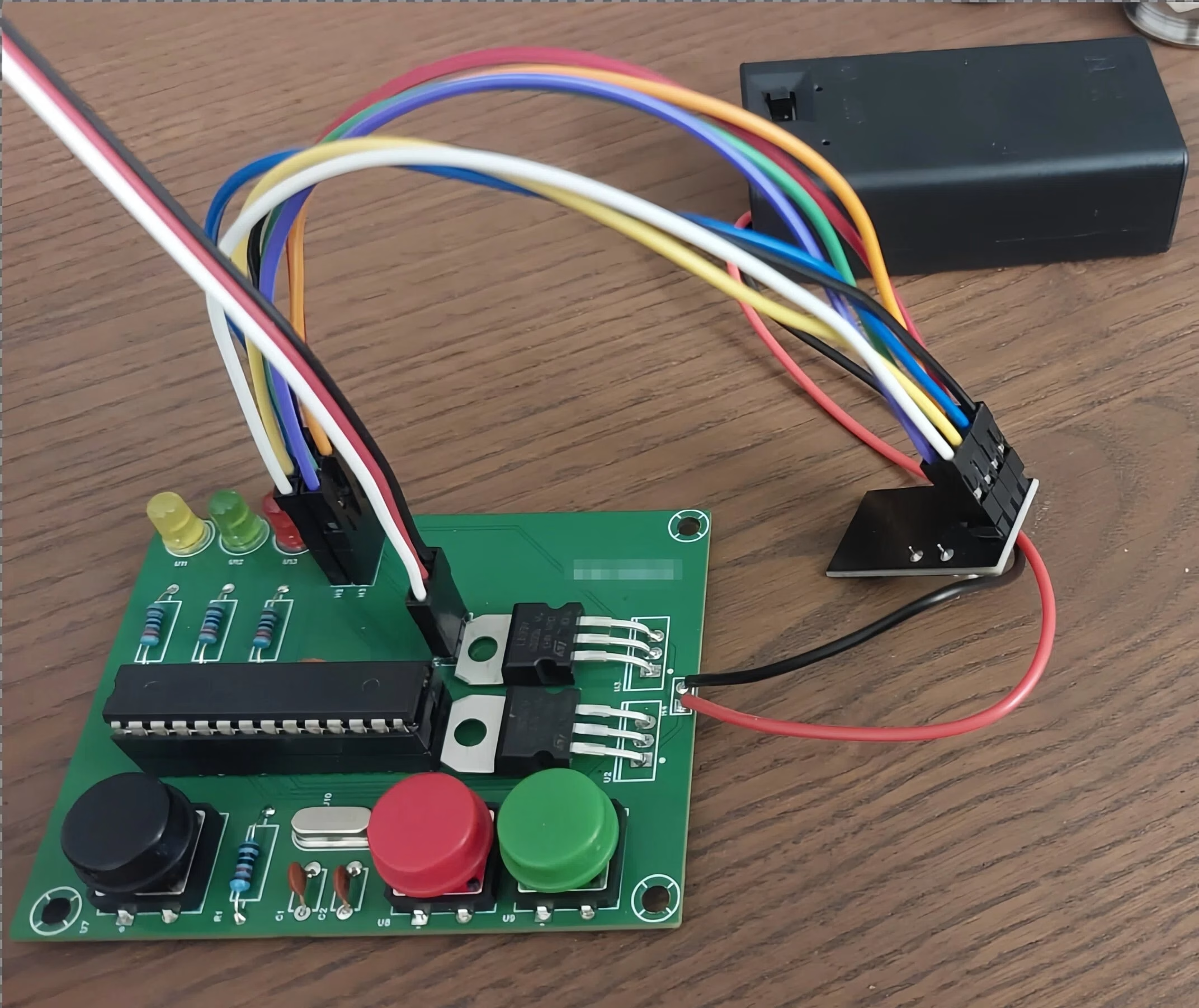
In certain special scenarios, standard jumper forms cannot meet requirements, giving rise to several unconventional solutions:
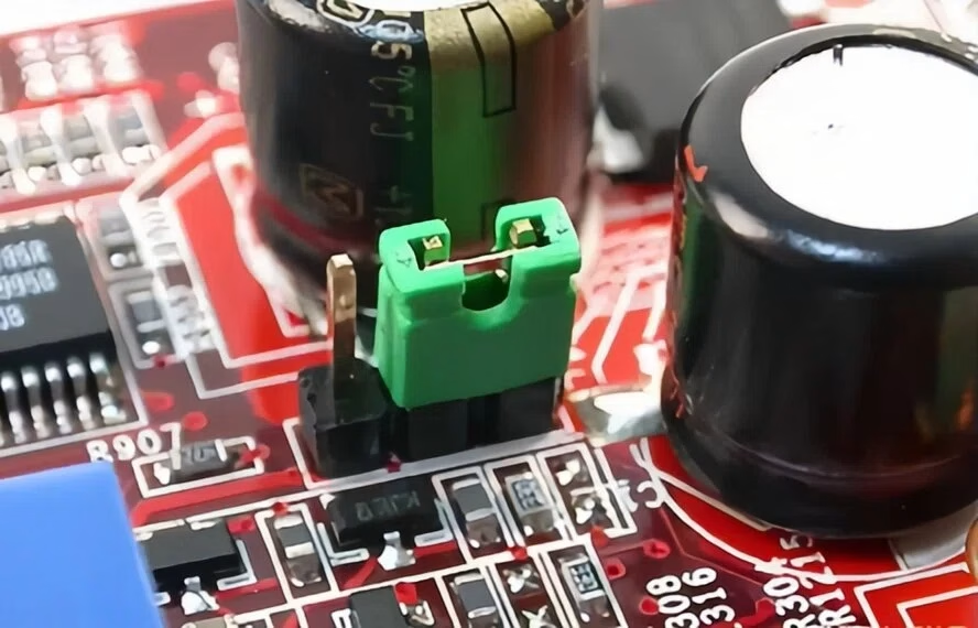
- Pin Headers with Shunts: Use 2.54mm pitch pin headers with shorting caps to implement jumper functionality. This structure is intuitive and reusable, widely applied on development boards like Arduino. The downside is larger space consumption, making it unsuitable for compact designs.
- Rigid-Flex PCB Jumpers: Use flexible PCB extensions as connecting bridges between rigid boards, upgrading the jumper concept from an “added component” to “structural integration.” This solution requires no soldered wires and offers high reliability, particularly suitable for compact devices requiring folding or curved installation.
- Coaxial Shielded Jumpers: In RF and high-speed circuits, ordinary jumpers can be disastrous for signal integrity. Coaxial cable-structured jumpers provide constant impedance and full shielding protection, minimizing electromagnetic interference.
3. Ten Core Design Rules for PCB Jumpers
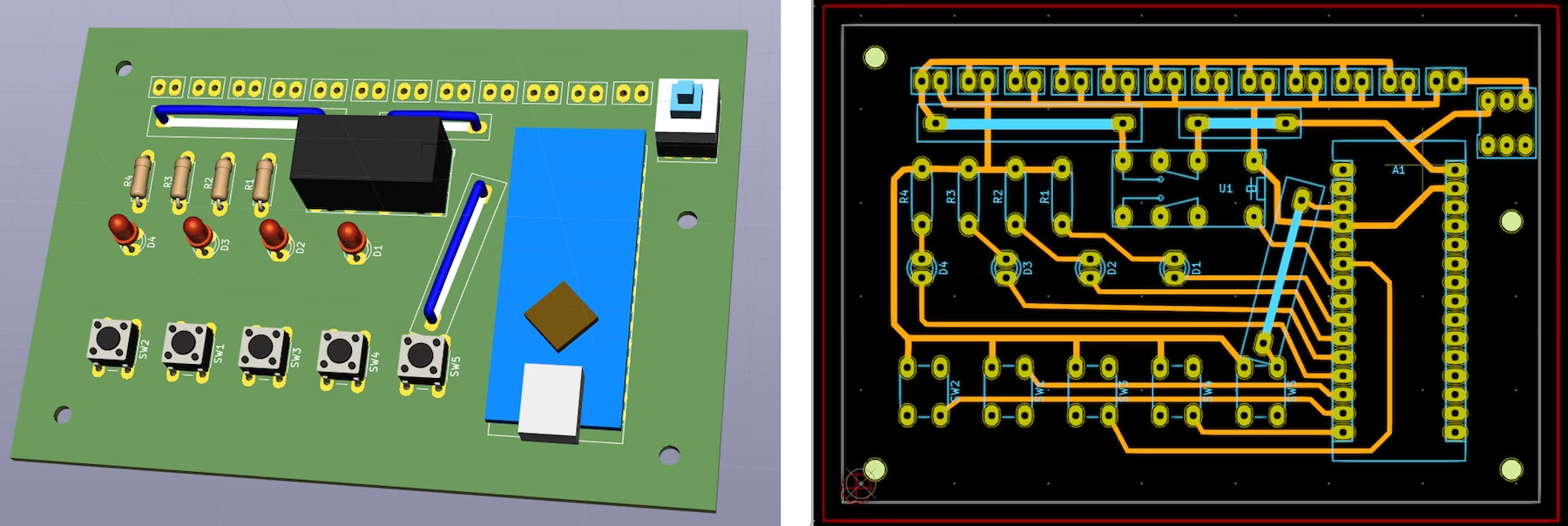
Jumpers may appear simple, but improper design can lead to signal degradation, reduced reliability, and even safety hazards. The following explains each of the ten jumper design rules with engineering practice in mind.
3.1 Prioritize Placement on the Component Side
Jumpers should be placed on the component side of the PCB whenever possible. The rationale is that the jumper itself is considered a “component,” and placing it on the same side as other major components enhances assembly integrity and maintainability. If jumpers are scattered on the solder side, they may interfere with wave soldering processes and are less convenient for visual 3.2 Route in an X-Y Orthogonal Manner
Jumper paths should follow straight lines along the X or Y direction, minimizing unnecessary bends. Orthogonal routing is not only neat and aesthetically pleasing but, more importantly, reduces wire length (thereby lowering parasitic inductance), simplifies layout review, and improves reliability. Every extra bend is a potential stress concentration point and failure source.
3.3 Control Height Above Board
The highest point of a jumper should not exceed 3.2mm above the PCB surface. Excessively tall jumpers are prone to being bumped during assembly or transport and may interfere with the enclosure. For scenarios requiring bridging over taller components, preformed jumpers or support posts should be used.
3.4 Limit Bare Conductor Length
The length of exposed conductor (uninsulated portion) should not exceed 12.7mm. Even shorter bare wires (<12.7mm) must meet minimum electrical clearance requirements. This rule is based on electrical safety considerations—excessively long exposed conductors increase the risk of accidental shorts.
3.5 Avoid Unused Pads and Test Points
Jumpers should not pass over unused component pads or test points. If layout constraints make this unavoidable, sufficient slack should be provided so the jumper can be moved if components need to be added later. This rule embodies design foresight—today’s jumper could become tomorrow’s modification obstacle.
3.6 Do Not Route Over Component Bodies or Leads
Jumpers must not pass over component leads, bodies, or heatsinks. Routing over components obstructs rework operations (soldering irons or hot air guns cannot easily access obscured solder joints). Routing over heatsinks may cause insulation to melt due to high temperatures, leading to shorts.
3.7 Provide Stress Relief and Control Bend Radius
Jumpers should include stress relief allowance to accommodate thermal expansion and mechanical vibration. The bend radius should be at least three times the conductor diameter, avoiding sharp bends. This is especially important in industrial or automotive environments—continuous vibration can cause tightly stretched jumper solder joints to fatigue and crack over time.
3.8 Insulate When Routing Through Plated Through-Holes
If a jumper must pass through a plated through-hole, the wire must be properly insulated. Alternatively, non-plated holes can be drilled specifically for wire routing, taking care not to damage inner layer traces.
3.9 Ensure Solder Joints Are Visible on Both Sides
When a jumper is soldered into a plated through-hole, the solder joint should be clearly visible on the opposite side. This requirement ensures joint integrity and inspectability—a solder joint that cannot be seen is a solder joint that cannot be verified.
3.10 Insulate and Bond Securely
After soldering, jumpers should receive necessary insulation protection (such as heat-shrink tubing). Subsequently, the jumper body should be bonded and fixed to the PCB surface using methods including: tape dots, quick-set adhesive, hot melt adhesive, or thermally bonding jumpers with a pre-applied thermoset adhesive coating using a specialized tool.
Supplementary Rule: For high-current scenarios, the current-carrying capacity of the jumper must be calculated. With 1oz copper thickness, a 1mm trace width carries approximately 0.5A. The AWG specification of the jumper directly determines its current limit. A 5A current requires an equivalent of at least 10mm trace width or multiple parallel wires. For high-voltage scenarios (>30V), creepage distance must also be considered—AC 220V safety spacing is recommended to be greater than 3mm.
4. Methods for Creating PCB Jumpers
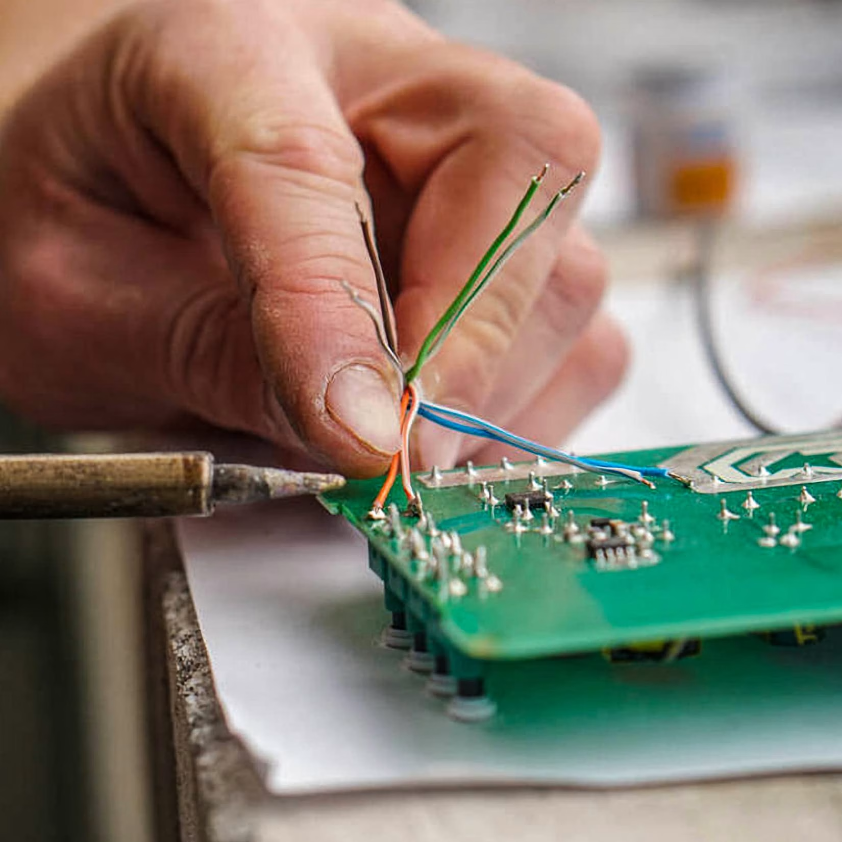
The creation of PCB jumpers varies by type. The following sections introduce the implementation methods for mainstream types.
4.1 Process for Physical Jumpers
The creation of physical jumpers involves both PCB design preparation and manual assembly phases.
Design Phase:
- In the PCB design software, place pads at the two nodes requiring jumper connection. The pad size should be at least twice the jumper wire diameter (e.g., ≥1mm pad for 0.5mm wire).
- Set the net attribute of the pads to ensure consistency between the schematic and PCB.
- Add jumper identifiers (such as J1, J2) and directional indicators on the silkscreen layer.
- If using insulated wire, define the jumper path between pads.
Assembly Phase:
- Cut the wire to the calculated length, including soldering allowance at both ends and height variations along the path.
- Strip the insulation from both ends of the wire, leaving approximately 2-3mm exposed.
- Form the wire to conform to the pre-defined path.
- Solder both ends, ensuring 360° wetting of the solder joint.
- Clean the solder joints if necessary, and secure the wire body with adhesive.
4.2 Configuration Methods for Jumper Pads
Configuration operations for jumper pads are relatively straightforward:
- Solder Bridge Connection: Heat both pads simultaneously with a soldering iron and feed an appropriate amount of solder to bridge them. Control the solder quantity carefully to avoid overflow onto adjacent pads.
- Copper Trace Cutting: For default-conducting copper jumpers, make cuts on both sides of the copper foil with a sharp blade, then peel off the middle copper foil or lift it by heating with a soldering iron. After cutting, verify the open circuit with a multimeter.
4.3 Soldering Zero-Ohm Resistor Jumpers
Soldering zero-ohm resistors is identical to soldering ordinary SMD components:
- Pre-tin one of the pads with solder.
- Use tweezers to position the resistor, heating the pre-tinned pad to secure one end of the resistor.
- Solder the other end, reheating the first end if necessary.
- Inspect the solder joints for bridging or cold solder defects.
5. Comparison Between PCB Traces and Jumper Wires
Jumper wires supplement traces; they do not replace them. Understanding the differences between the two helps in making correct design choices.
| Comparison Dimension | PCB Trace | Jumper Wire |
| Path Length | Can route arbitrarily across the entire board | Suitable for short connections, typically ≤50mm |
| Flexibility | Cannot be changed after manufacturing | Adjustable, removable |
| Impedance Control | Precisely controllable, suitable for high-speed signals | Difficult to control precisely, unsuitable for impedance-sensitive signals |
| Signal Frequency | Supports multi-Gbps high-speed signals | Suitable for low-speed signals; high-frequency limited |
| Current-Carrying Capacity | Can be increased by thicker copper and wider traces | Limited by wire gauge; high current requires special design |
| EMI Performance | Good shielding achievable with ground planes | Prone to becoming interference source or receiver |
| Reliability | Co-lifetime with PCB; no additional failure points | Solder joint + wire structure; fatigue and fracture risks exist |
| Cost | High cost for additional layers | Low unit cost, but manual soldering required |
| Manufacturability | Fully automated production | Partial manual work; affects throughput |
Decision Guidance: For high-speed signals (clocks, differential pairs, RF), high-current main paths, and high-reliability requirement scenarios, prioritize PCB traces. For unavoidable single-layer board crossings, configuration options, prototype validation, and defect repair scenarios, judiciously use jumper wires.
6. Typical Applications of PCB Jumpers
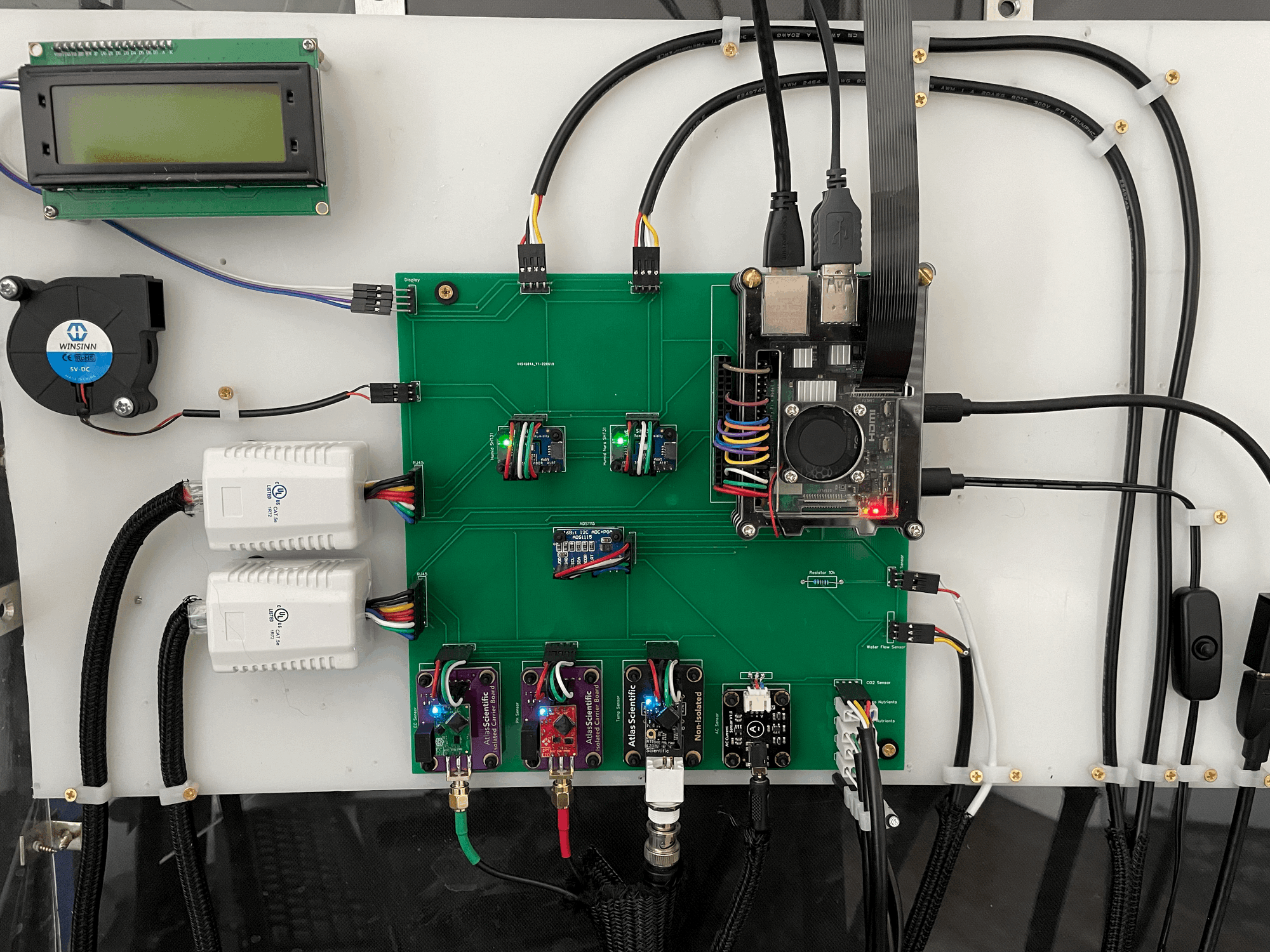
6.1 Single-Layer Board Routing Solutions
Single-layer boards have only one copper layer. When traces cross, jumpers are the only solution. The typical approach is to break a trace and use a top-side jumper to bridge over the conflict area, creating an “aerial overpass.” Consumer electronics such as TV mainboards extensively use this technique to achieve complex circuit functionality at low cost.
6.2 Circuit Configuration and Mode Selection
By pre-designing jumper pads or zero-ohm resistor positions, the same PCB can adapt to multiple configurations: power supply voltage selection (5V/3.3V), communication protocol switching (UART/SPI/I2C), functional module enabling/disabling, and hardware version differentiation. This design approach allows a single hardware platform to cover multiple product models, significantly reducing development and inventory costs.
6.3 Prototype Validation and Rapid Iteration
During prototype development, jumpers (especially pin headers with shunts) allow engineers to quickly try different connection schemes without waiting for a new PCB revision. The ecosystem of development platforms like Arduino is built precisely on this jumper flexibility.
6.4 Design Defect Repair and Circuit Modification
When a PCB contains design defects, jumpers are a cost-effective remedial measure. Jumpers can be categorized into three types: design jumpers planned during the design phase, modification jumpers added due to design changes, and defect correction jumpers applied after manufacturing.
6.5 Test Point Access and Debugging
On PCBs lacking dedicated test points, temporary jumpers can be soldered to bring internal signals out for oscilloscope or logic analyzer debugging. This method requires no PCB damage and can be removed once debugging is complete.
6.6 High-Current Path Reinforcement
In power circuits where PCB copper traces cannot meet current-carrying requirements, jumpers can be added in parallel as reinforcement. KOA metal plate jumpers of the TLRZ series feature resistance as low as 0.5mΩ and rated current up to 50A, far exceeding the capacity of comparably sized PCB copper.
7. FAQs
Q1: What is the difference between a jumper wire and a flying wire?
A jumper wire is a connection component proactively planned during the design phase, with pre-designed pads and clear specifications. A flying wire is a temporary remedial measure during repair or debugging, typically without pre-designed positions. From an engineering management perspective, a jumper is “part of the design,” whereas a flying wire is a “patch for a problem.”
Q2: Can jumpers be used on high-speed signals?
Not recommended. Jumpers make it difficult to control impedance, and parasitic inductance can affect signal quality. High-speed signals (DDR, SerDes, RF, etc.) should prioritize PCB traces, using ground planes and differential pair design to ensure signal integrity. If jumper use is unavoidable, keep the length as short as possible (<5mm) and consider shielding measures.
Q3: How to select the wire gauge for a jumper?
Wire gauge selection depends on the current passing through. General principles: 100mA can use 0.2mm²; 1A requires ≥0.5mm². For signal lines such as GPIO, 22AWG or thicker is recommended. For high-current scenarios, consult wire gauge current rating tables and reserve a 20% safety margin.
Q4: Is the resistance of a zero-ohm resistor truly zero?
No. The actual resistance of a zero-ohm resistor is typically below 50mΩ for rectangular chip types, and even lower for metal plate types. This tiny resistance is negligible in most scenarios, but voltage drop and heat dissipation still need consideration when passing large currents.
Q5: How to calculate jumper wire length?
Jumper length = straight-line distance between the two pads + height variation along the path (climbing height to bridge components) + soldering allowance (approximately 2-3mm per end) + slack allowance. For right-angle connections, horizontal and vertical segments must be calculated separately.
Q6: Do jumpers need insulation?
It depends on the scenario. Low-voltage, low-speed signals can use bare wire within controlled lengths. When bridging over components or passing through dense areas, insulated wire should be used. High-voltage signals (>30V) must be insulated. For mass production products, it is recommended to uniformly use insulated jumpers to avoid accidental shorts.
8. Summary
PCB jumpers, though seemingly insignificant, are key to resolving routing conflicts and achieving configuration flexibility. From physical wires to zero-ohm resistors to software-controlled switches, their forms evolve, but the core mission remains the same. Proper usage requires balancing flexibility with discipline—the ten rules in this article serve this foundation—and clearly distinguishing the applicable boundaries between jumpers and traces is a hallmark of mature design. Future technologies such as carbon nanotubes, graphene, and MEMS switches may redefine jumper technology, but understanding their electrical principles and reliability characteristics will remain essential knowledge for hardware engineers.








