
A Guide to Every Layer Interconnect(ELIC) for HDI PCB

Table of Content
In the relentless pursuit of smaller, faster, and more powerful electronic devices, High Density Interconnect(HDI) Printed Circuit Boards(PCBs) have become indispensable. As components continue to shrink and their numbers multiply, the challenge of connecting them all within a limited physical space intensifies. This demand for extreme miniaturization and enhanced performance has driven constant innovation in HDI technology, culminating in the most sophisticated approach yet: Every Layer Interconnect (ELIC) PCBs.
ELIC technology isn’t just an incremental improvement; it’s a revolutionary design and manufacturing methodology that allows for unparalleled interconnect density and routing flexibility. By enabling connections between any and all layers of a multilayer PCB stackup, ELIC overcomes the limitations of traditional HDI, making it possible to design and produce cutting-edge electronics that were once considered impossible. This guide will delve into the intricacies of ELIC PCB, exploring its structure, advantages, manufacturing process, and its critical role in shaping the future of high-tech devices.
1. What is Every Layer Interconnect(ELIC) PCB?
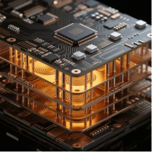
Every Layer Interconnect(ELIC) is an advanced form of High Density Interconnect(HDI) PCB technology that takes interconnect density to its absolute peak. At its core, ELIC allows for microvias to be extended throughout the entire PCB stackup, enabling signals to route on high density interconnects between any set of layers in the PCB, not just adjacent ones. This contrasts sharply with standard HDI constructions, which often rely on a combination of blind, buried, and through-hole vias, typically connecting only specific layers or groups of layers.
The fundamental idea behind ELIC is straightforward: total connectivity. Imagine a multi-story building where you can build an elevator shaft between any two floors, regardless of whether they are directly adjacent. This “any-to-any layer” routing capability is what sets ELIC apart. It means that a trace on layer 1 can connect directly to a trace on layer 6, without needing to pass through intervening layers via a series of sequentially stacked vias. This level of design flexibility is crucial for managing the increasingly complex circuit connectivity and component layouts found in modern advanced electronics.
Also known as “any-layer HDI”, ELIC utilizes sophisticated microvia technology to achieve this universal connectivity. These microvias are typically laser-drilled, offering extremely small diameters, which significantly conserves board space. The ability to place these tiny connections anywhere in the stackup provides designers with immense freedom, reducing overall PCB size and weight while boosting electrical performance.
2. ELIC vs. Standard HDI: A Fundamental Shift
To fully appreciate the significance of ELIC, it’s helpful to understand its distinctions from conventional HDI PCB structures. While both aim to increase interconnect density, ELIC represents the ultimate evolution in this area. Standard HDI PCB stackups, as defined by IPC-2226 standards, often employ core (buried) vias, through-hole vias, and/or blind/buried microvias to facilitate trace routing into fine-pitch BGA components. These methods, while effective, still impose certain routing constraints.
For instance, standard HDI might use skip vias on the surface layer in addition to standard blind/buried microvias to allow BGA breakouts to access inner layers. However, these connections are typically sequential and layer-dependent. ELIC, on the other hand, breaks these traditional barriers by allowing truly arbitrary layer-to-layer connections. This capability directly impacts routing efficiency and signal integrity.
| Feature | Standard HDI PCB | Every Layer Interconnect(ELIC) PCB |
| Via Type | Blind, Buried, Through-hole, Skip Vias | Stacked Microvias(Laser-Drilled) |
| Connectivity | Sequential, specific layer-to-layer connections(e.g., L1-L2, L1-L3, L2-L3) | Any-to-any layer interconnection(e.g., L1-L6 directly) |
| Interconnect Density | High | Highest Possible |
| Routing Flexibility | Good, but with limitations | Unparalleled, maximum design freedom |
| Complexity | High | Most Complex |
| Manufacturing Process | Advanced | Highly Advanced(Laser drilling, Plasma etching, advanced materials) |
| Typical Applications | Smartphones, laptops, automotive | High-end smartphones, aerospace, medical implants, AI hardware |
3. The Unmatched Advantages of ELIC Technology
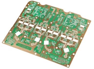
The capabilities of ELIC PCBs translate into several profound advantages for modern electronics design and manufacturing:
Unparalleled Interconnect Density
ELIC’s primary benefit is its ability to achieve the highest possible interconnect density. By allowing microvias to connect any two layers, designers can utilize every available layer efficiently. This is crucial for accommodating the increasing number of pins on fine-pitch BGA components and complex integrated circuits, making it possible to pack more functionality into a smaller footprint. This density is a key enabler for miniaturization, reducing the overall size and weight of electronic devices.
Enhanced Design Flexibility
The “any-layer” routing capability liberates designers from the constraints of traditional via structures. This newfound design flexibility allows for more optimized component placement and trace routing, simplifying complex layouts and potentially reducing design cycles. Engineers can route signals between layers without needing to “staircase” vias through multiple intermediate layers, leading to shorter trace lengths and fewer routing bottlenecks. This is particularly beneficial for complex multi-layer designs.
Superior Signal Integrity
With high-speed PCBs becoming the norm, maintaining excellent signal integrity is paramount. ELIC technology contributes to this by enabling shorter signal paths due to its direct layer-to-layer connections. Shorter traces mean less signal attenuation, reduced impedance discontinuities, and lower electromagnetic interference(EMI). This translates into faster signal transmission, improved reliability, and better performance for demanding applications like high-frequency data processing and communication systems.
Miniaturization and Performance
ELIC technology directly supports the trend of miniaturization without compromising performance. By maximizing interconnect density and optimizing routing, ELIC PCBs allow for smaller board sizes, which is critical for compact portable devices. Moreover, the improved signal integrity and thermal management(due to denser stacking and optimized material choices) ensure that these smaller devices don’t just shrink in size but also boost their operational speed and reliability.
4. Designing an ELIC PCB Stackup: Key Considerations
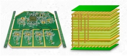
Designing an ELIC PCB stackup is a meticulous process that requires deep understanding of advanced materials, manufacturing capabilities, and signal integrity principles. The “innocuous allowance” of extending microvias throughout the entire stackup places significant constraints on the material sets and the manufacturing processes used to build the PCB.
Key considerations include:
- Material Selection:ELIC PCBs often require specialized dielectric materials with controlled impedance properties, excellent thermal stability, and low Dk/Df(dielectric constant/dissipation factor) for high-frequency applications. The materials must also be compatible with the advanced laser drilling and plasma etching processes.
- Layer Count and Thickness:While ELIC allows for higher density, careful consideration of the overall layer count and individual layer thicknesses is vital for managing impedance and thermal performance. Thinner layers and higher layer counts are common in ELIC designs.
- Via Design:Precise microvia design, including aspect ratio, diameter, and pad size, is critical. The vias must be reliably formed and filled to ensure robust electrical connections and prevent voids.
- Thermal Management:With higher component density, effective thermal management becomes crucial. Designers must plan for heat dissipation, potentially incorporating thermal vias or specialized substrate materials.
- Impedance Control:Maintaining consistent impedance for high-speed traces throughout the complex ELIC stackup is a major challenge. Careful trace width, spacing, and dielectric thickness calculations are essential.
5. The ELIC PCB Manufacturing Process
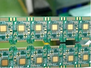
The fabrication of ELIC PCBs is significantly more complex and precise than that of conventional PCBs, demanding advanced manufacturing techniques and stringent process control. It involves a multi-stage buildup process, essentially constructing the PCB layer by layer.
Advanced Techniques for Precision
The core of ELIC manufacturing lies in the sequential buildup of layers, typically involving:
1) Core Preparation: Starting with a central core layer, often a thin laminate.
2) Dielectric Layer Application: A thin layer of prepreg or build-up material is applied.
3) Laser Drilling: Microvias are precisely drilled using advanced laser drilling technology. These lasers can create extremely small holes(typically less than 150 microns in diameter) with high accuracy. This step is critical for forming the “every layer” connections.
4) Desmear and Metallization: After drilling, a desmear process(often using plasma etching) is performed to clean the via holes and remove resin residue, ensuring a clean surface for metallization. This is followed by electroless copper deposition and electroplating to metallize the microvias.
5) Patterning and Etching: Photolithography is used to create the circuit patterns, which are then etched onto the copper layer.
6) Lamination and Stacking: The processed layer is then laminated with another dielectric layer and copper foil , and the process of laser drilling, desmear, metallization, and patterning is repeated for each subsequent layer, building the board up sequentially. This sequential lamination is what allows for the creation of stacked microvias that connect any two layers.
7) Via Filling: Microvias are typically filled with conductive or non-conductive epoxy to provide structural integrity, prevent trapping of plating chemicals, and ensure a flat surface for subsequent layer processing.
This iterative process, requiring extreme precision at each step, allows for the creation of robust and reliable connections throughout the entire PCB stackup.
6. Real-World Applications of ELIC PCBs
Given their ability to maximize interconnect density and provide unparalleled design flexibility, ELIC PCBs are indispensable in a range of advanced electronic devices where space is at a premium and performance is critical. Their adoption is widespread in sectors pushing the boundaries of technology:
- High-End Smartphones and Wearables:The constant demand for thinner, lighter, and more feature-rich mobile devices makes ELIC a perfect fit. It allows for the integration of more components, memory, and processing power within shrinking form factors.
- Aerospace and Defense:Mission-critical applications in satellites, avionics, and defense systems benefit from ELIC’s reliability, reduced weight, and superior signal integrity, particularly in harsh environments.
- Medical Devices:Compact, high-performance medical implants, diagnostic equipment, and portable health monitoring devices rely on ELIC for their intricate circuitry and small size.
- Artificial Intelligence(AI) and High-Performance Computing(HPC):Processors and modules designed for AI acceleration and HPC often require extremely dense interconnects to manage vast amounts of data at high speeds, making ELIC an ideal solution.
- Automotive Electronics:Advanced driver-assistance systems(ADAS), infotainment systems, and autonomous driving platforms require complex, reliable, and space-efficient PCBs, areas where ELIC excels.
- Network and Communication Infrastructure:High-speed routers, switches, and other communication equipment benefit from the enhanced signal integrity and routing efficiency offered by ELIC.
7. ELIC PCB FAQs
Question 1: What is the main advantage of ELIC over standard HDI?
The primary advantage is its “any-to-any layer” connectivity, achieved through stacked microvias. This offers unparalleled interconnect density and design flexibility, allowing signals to connect directly between any two layers, unlike standard HDI which has more restricted, sequential layer connections.
Question 2: Are ELIC PCBs more expensive to manufacture?
Yes, ELIC PCBs are generally more expensive due to the highly advanced manufacturing processes involved, such as sequential laser drilling, plasma etching, precise metallization, and specialized material sets. The increased complexity and precision required contribute to higher production costs.
Question 3: What types of applications benefit most from ELIC technology?
ELIC PCBs are ideal for applications requiring extreme miniaturization, high-speed performance, and complex circuit integration. This includes high-end smartphones, medical implants, aerospace electronics, AI hardware, and other high-performance computing devices where space is limited and signal integrity is critical.
Question 4: How does ELIC improve signal integrity?
ELIC improves signal integrity by enabling shorter and more direct signal paths between layers. This reduces signal attenuation, minimizes impedance discontinuities, and lowers electromagnetic interference(EMI), leading to faster and more reliable signal transmission, which is crucial for high-speed PCBs.
8. Summary
Every Layer Interconnect(ELIC) technology represents the pinnacle of High Density Interconnect(HDI) PCB innovation, fundamentally reshaping what’s possible in modern electronics design. By extending microvias throughout the entire PCB stackup, ELIC enables truly “any-to-any layer” connections, providing an unparalleled increase in interconnect density and design flexibility. This allows for the integration of more complex components, such as fine-pitch BGA components, into ever-shrinking footprints, driving forward the trend of miniaturization without sacrificing performance.
The manufacturing process for ELIC PCBs is sophisticated, relying on advanced techniques like sequential laser drilling, plasma etching, and specialized materials to build up the board layer by layer with extreme precision. The resulting PCBs offer superior signal integrity, making them ideal for high-speed PCBs and high-frequency applications where performance and reliability are paramount. From the latest smartphones and wearables to critical aerospace and medical devices, ELIC PCBs are the foundational technology enabling the next generation of advanced electronics.
OrinewPCB has focused as a one-stop PCB assembly manufacturer from PCB Manufacturing to Electronic Components Sourcing to PCB Assembly to Test to Program IC for more than 14 Years with reliable quality and fastest delivery for global clients.








