Power Management Unit (PMU) PCB Design Guide

Table of Content
- 1. Fungsi Teras dan Komposisi PMU
- 2. Garis Panduan Susun Atur PCB PMU
- 3. Garis Panduan Penghalaan PCB PMU
- 4. Reka Bentuk Pelesapan Haba
- 5. Cadangan Susunan PCB Berbilang Lapisan
- 6. Masalah dan Penyelesaian Reka Bentuk Biasa
- 7. Perkara Utama Pengesahan dan Pengujian Reka Bentuk
- 8. Soalan Lazims
- 9. Ringkasan
The Power Management Unit (PMU) is the core of electronic products such as smartphones and industrial equipment. It converts electrical energy into different voltages and currents required by the system, and handles power distribution and protection. Its performance directly determines the device’s battery life, stability, and safety.
A well-designed PMU PCB achieves efficient conversion, precise voltage regulation, noise suppression, and reliable heat dissipation. Poor layout can cause excessive ripple, EMI issues, chip overheating, or even damage.
This guide starts from the core functions of the PMU and systematically explains layout, routing, heat dissipation, and common mistakes. It helps engineers master practical methods for designing robust and efficient power systems.
1. Core Functions and Composition of the PMU
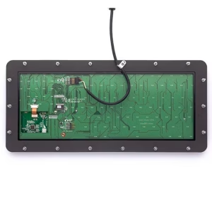
1.1 Core Functions of the PMU
As the “brain” and “heart” of the power system, the PMU integrates multiple power management and control functions:
- Power Management: Provides accurate and appropriate voltage and current to different functional modules in the system, such as CPU, memory, RF circuits, and sensors.
- Power Path Switching: Achieves seamless switching between battery power and external adapter power, preventing device restart or data loss during power source changes.
- Battery Management: Monitors battery level, voltage, and temperature in real time. Implements smart charging strategies (such as trickle, constant current, constant voltage charging) to prevent overcharge and over-discharge, thus extending battery life.
- Power Optimization: Dynamically adjusts power supply status based on system load. Enters low-power mode during standby or light load, and provides sufficient current when high performance is needed, optimizing overall energy efficiency.
- Hardware Protection: Continuously monitors input/output voltage, current, and chip temperature. When abnormalities (such as overvoltage, overcurrent, overtemperature) are detected, it triggers protection mechanisms (such as reducing power, shutting down output, or disconnecting the power supply) to ensure system safety.
1.2 Typical Components of a PMU
A complete PMU typically consists of internal integrated modules and necessary external components:
- DC-DC ConverterModule: Usually a switching power supply (Buck, Boost, or Buck-Boost). Used for high-efficiency voltage conversion to power main functional modules.
- LDO (Low Dropout) LinearRegulator: Provides stable voltage with low noise and high Power Supply Rejection Ratio (PSRR). Very suitable for sensitive circuits such as analog circuits, RF circuits, and phase-locked loops.
- Control Circuit: Handles power sequencing, voltage/current monitoring, status register management, and communication with the main chip (such as via I²C or SPI interface).
- Protection Circuit: Integrates Over-Voltage Protection (OVP), Over-Current Protection (OCP), Over-Temperature Protection (OTP), and Under-Voltage Lockout (UVLO) to improve system robustness.
- External Filtering Network: Includes ceramic capacitors, electrolytic capacitors, inductors, and ferrite beads at input and output. Used to filter switching ripple and noise.
- Auxiliary Function Modules: May include battery fuel gauge, charging control circuit, LED driver, etc.
2. PMU PCB Layout Guidelines
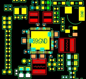
Good layout is the foundation of successful PCB design. For PMUs, the goals of layout are to optimize power loops, reduce noise coupling, and ensure good heat dissipation. The recommended layout sequence is: handle the DC-DC section first, then place LDOs, and finally place control circuits.
2.1 Layout Key Points for DC-DC Converters
DC-DC switching power supplies are the main source of noise in a PMU. Their layout is critical:
- Place First: First determine the positions of the DC-DC converter chip and its key external components such as inductors and input/output capacitors.
- Inductor Layout: The inductor is the core energy storage component. Ensure the connection between the inductor and the chip’s switch pin (SW/LX) is as short and wide as possible to reduce parasitic inductance and resistance.
- Orthogonal Placement of Adjacent Inductors: If the PMU contains multiple DC-DC converters and their inductors are placed side by side, rotate adjacent inductors 90 degrees (orthogonal) to reduce magnetic field coupling and crosstalk.
- Keep-Out Area Under Inductor: Do not place any critical signal lines or sensitive devices directly under the inductor. The inductor’s magnetic field can interfere with nearby signals. Also, avoid routing sensitive traces near the inductor’s pads.
- Input High-Frequency Filtering Capacitor: Identify the “high di/dt loop” (hot loop) of the DC-DC converter. The high-frequency decoupling capacitor in this loop (typically 0.1µF~10µF X5R/X7R ceramic capacitor) must be placed very closeto the chip’s input pin (VIN) and ground pin (PGND). Connect them with short, wide traces or inner layer planes, avoiding vias in between.
2.2 Handling the Switch Node (SW) and High-dV/dt Nodes
The voltage at the switch node switches rapidly between the input voltage and ground. The voltage change rate (dV/dt) is extremely high, making it a primary source of EMI radiation.
- Minimize Node Area: Without affecting heat dissipation, minimize the copper area of the switch node (the connection connecting the chip’s SW pin, one end of the inductor, the bootstrap circuit, etc.) to reduce the antenna effect.
- Shielding Layer: In multi-layer board designs, it is recommended to place a complete ground plane on the layer directly below the switch node to provide additional isolation and suppress noise propagation.
2.3 Layout Key Points for LDOs
The layout for LDOs is simpler than for DC-DC converters, but there are still considerations:
- Placement Order: Place LDOs after completing the DC-DC section layout.
- Output Capacitor: The LDO’s output capacitor (especially low-ESR ceramic types) should be placed very closeto the LDO’s output pin and ground pin to ensure loop stability.
- Heat Dissipation Consideration: For higher-power LDOs, the bottom thermal pad needs vias connected to the ground plane and possibly a copper area for heat spreading.
- Backside Placement: When space is limited, smaller capacitors can be placed on the backside of the PCB, connected to the LDO’s pins through vias.
2.4 Overall Layout Optimization
- Functional Partitioning: Physically separate the power section (DC-DC converters, inductors, large capacitors) from the small-signal control section (feedback resistors, compensation networks) to prevent power noise from coupling into the control circuits.
- Maintain Adequate Spacing: Leave sufficient space between components for later routing, heat dissipation, and debugging. In particular, reserve space around thermal pads for thermal vias.
- Final Adjustment: After placing all major components, perform overall fine-tuning and optimization. Check space utilization and critical paths.
3. PMU PCB Routing Guidelines
Routing must follow three major principles: sufficient current carrying capacity, shortest return path, and minimal interference. It is recommended to fan out the DC-DC power section first.
3.1 Power Trace Routing
- Trace Width Calculation: Power traces (input/output main paths) carry high currents. Insufficient width causes temperature rise and voltage drop. An empirical formula can be used: Trace width (mil) ≈ Current (A) × (10~20) / (Copper weight (OZ)). For example, for 5A current on 1OZ copper, a trace width of at least 120 mil is recommended.
- Short and Wide: Traces from the DC-DC output pin to the inductor, and from the inductor to the output capacitor, should be short, wide, and straight to minimize parasitic resistance and inductance.
- Via Placement: Add vias to connect to power planes only after the last output filter capacitor. The number of power vias should match the number of ground vias to ensure balanced current return paths.
3.2 Input and Output Loop Routing
- Input Loop: The input current path should be as short and wide as possible. The GND terminal of the input capacitor should connect to the chip’s PGND (power ground) by the shortest path.
- High-Frequency Decoupling Capacitor: The routing for the input high-frequency decoupling capacitor is critical. Its power and ground terminals should connect directly to the chip’s VIN and PGND pins via short, wide traces or inner layer areas. If vias are necessary, place them very close to the capacitor pads.
3.3 Feedback (FB) and Control Signal Routing
- Close to Chip: The feedback resistor divider network and related compensation network components must be placed very closeto the chip’s feedback pin (FB).
- Away from Noise Sources: The feedback trace from the divider resistor output to the chip’s FB pin must be routed away from inductors and switch nodes, and should not run parallel to high-current power traces. A thin trace (~10 mil) with a complete ground plane as reference is recommended.
- Avoid Interference: Analog ground (AGND) and power ground (PGND) typically need to be separated. They should be connected at a single point, usually under the chip’s thermal pad or at a specific low-impedance point.
3.4 Via Usage
- Thermal Vias: Add multiple vias denselyon the chip’s exposed thermal pad. Connect them to the ground plane or a dedicated copper area for heat spreading. Vias can be tented or filled with copper to enhance thermal conductivity.
- Fan Out All Netted Pads: All pads that have nets should be fanned out to ensure signal integrity.
- Quantity Matching: The number and position of power vias should be coordinated with the ground return vias to avoid creating large current loops.
3.5 Routing for Multiple Power Supplies
When multiple power supplies share one input source and operate asynchronously, separate their input power traces to prevent common-mode noise from propagating through the input paths and ground.
4. Heat Dissipation Design
The heat dissipation design of the PMU directly affects the long-term reliability of the system.
- Use Copper for Heat Spreading: Use wide copper traces or inner layer power/ground planes to conduct heat from power devices to other areas of the PCB.
- Add Thermal Vias: Use many vias under the chip’s thermal pad, MOSFETs, and inductors to connect to ground layers or dedicated thermal layers.
- Consider System Airflow: During system layout, try to place the PMU near the air exhaust vent. Ensure that tall components (like electrolytic capacitors, large inductors) do not block the heat dissipation path from shorter, heat-generating active devices (like the PMU chip itself).
- Thermal Monitoring: Ensure the chip’s temperature sense pin and thermistor (NTC) are laid out reasonably to accurately reflect the actual junction temperature.
5. Multi-Layer PCB Stack-up Recommendations
In multi-layer boards, a proper stack-up design is critical for controlling EMI and ensuring signal integrity.
- Recommended Stack-up: Top Layer – Power and signals; Inner Layer 1 – Complete ground plane (GND); Inner Layer 2 – DC power plane (e.g., main system voltage VCC or internal power); Bottom Layer – Control signals.
- Shielding and Isolation: Sandwichcritical small-signal layers between a ground plane and a DC power plane for effective shielding. Do not place a small-signal layer directly adjacent to a high-current power layer, as this introduces significant capacitive coupling noise.
- Ground Plane Integrity: Maintain the integrityof the ground plane (GND). Avoid splitting it or routing traces on it if possible. If traces are necessary, ensure they run in the same direction as the high current on the power layer and are as short as possible.
6. Common Design Problems and Solutions
| Common Problem | Root Cause | Solution |
| Excessive Output Voltage Ripple | Improper output capacitor filtering; Feedback trace interference; Poor input capacitor layout | Check if output capacitor is close to chip and use low-ESR type; Check if feedback trace is away from inductor and SW node; Optimize input high-frequency cap layout |
| Poor Power Efficiency | Insufficient power trace width; High inductor DCR; Thermal shutdown due to poor heat dissipation | Widen power traces; Choose inductor with lower DCR; Check thermal vias and airflow, add heatsink if necessary |
| System EMI Exceeds Limits | Excessively large switch node (SW) copper area; Excessive high di/dt loop area | Minimize SW copper area while maintaining thermal performance; Relayout input capacitor to be very close to chip, minimizing the high-frequency loop |
| Chip Overheating | Insufficient thermal vias; Small copper area for heat spreading; Poor system airflow | Increase thermal via density; Enlarge copper area connected to thermal pad; Re-evaluate system airflow, ensure PMU is in the downstream air path |
| Poor Load Regulation / Dynamic Response | Feedback path too long; Output capacitor too far from load | Shorten feedback trace; Place bulk output capacitors (especially high-frequency caps) close to the load |
7. Design Verification and Testing Key Points
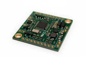
- No-Load/Full-Load Test: Measure whether the output voltage is within specification and whether ripple and noise meet load requirements.
- Efficiency Test: Measure input/output power under typical and full load conditions to calculate conversion efficiency.
- Thermal Imaging: After long-term operation under full load, use a thermal imager to check whether the temperatures of the PMU chip, inductor, and MOSFETs are within rated limits.
- Dynamic Load Response: Use an electronic load to simulate load transients and observe whether output voltage overshoot and undershoot are within allowed limits.
- EMI Pre-test: Use a near-field probe to scan the PCB, identify potential radiation hotspots, and ensure compliance with relevant standards.
8.FAQs
Q1: Why does my DC-DC circuit voltage drop significantly under heavy load?
A: It may be due to excessive impedance on the power path. Check whether the trace width on the input/output main paths is sufficient and whether too many vias are used (they add resistance). Additionally, an inductor with high DCR can also cause voltage drop.
Q2: Can feedback resistors be placed on the backside of the PCB?
A: Yes. However, after connection through vias, ensure the trace to the chip’s FB pin remains as short as possible and is kept away from noise sources. Also, the vias themselves should not introduce excessive parasitic parameters.
Q3: What are the different requirements for shielded vs. unshielded inductors in PCB design?
A: Shielded inductors (molded, semi-shielded) have lower magnetic flux leakage and cause less interference to other components, but it is still recommended not to route sensitive signals directly under them. Unshielded inductors have high leakage flux. A large “clean area” must be maintained around them, and no signal traces should be placed directly under or immediately next to them.
Q4: How should I handle multiple grounds (AGND, PGND) in a PMU?
A: The basic principle is single-point connection. Physically separate the noisy power ground (PGND) from the clean analog ground (AGND) on the PCB. Finally, connect them together at a single low-impedance point, typically under the chip’s exposed thermal pad or through a dedicated copper area or via. Avoid randomly mixing the two grounds.
Q5: My PMU board makes audible noise during operation. What could be the cause?
A: This is often caused by Pulse Skipping Mode (PSM) during light load or mechanical vibration of the inductor within the audio frequency range. It could also be due to the piezoelectric effect of ceramic capacitors. Try adjusting the switching frequency (if adjustable), increasing the output capacitance, or modifying the light load mode settings.
Q6: My PMU chip recommends using X5R/X7R capacitors. Can I use Y5V or standard electrolytic capacitors instead?
A: Not recommended. X5R/X7R ceramic capacitors have good capacitance stability over temperature and have low ESR (Equivalent Series Resistance) and low ESL (Equivalent Series Inductance), making them very suitable for filtering and decoupling in switching power supplies. Y5V capacitors have very poor capacitance stability with temperature and voltage. Ordinary electrolytic capacitors have high ESR, are not suitable for high-frequency filtering, and will cause increased ripple and heat generation.
9. Summary
PMU PCB design is a systems engineering task that integrates circuit principles, component characteristics, electromagnetic field theory, thermodynamics, and mechanical structure. Successful PMU design requires balancing multiple goals of high efficiency, low noise, good thermal performance, and reliability within a limited PCB space.
This guide emphasizes the following core principles:
- Layout First: Prioritize and optimize power loops. Do not route sensitive traces under inductors.
- Short Path Principle: Ensure critical paths are shortest and widest.
- Partition and Isolate: Physically separate the noisy power section from the sensitive control and feedback section. Use reference planes for shielding.
- Prioritize Thermal Management: Consider heat dissipation starting from the layout phase. Use thermal vias, copper areas, and system airflow appropriately.
- Simulate and Verify: Use simulation tools for preliminary evaluation during the design phase, and perform thorough electrical, thermal, and EMI testing during the prototyping phase.
By mastering and applying these principles, engineers can avoid common pitfalls and design high-performance, stable power systems that pass stringent market tests. As electronic devices move towards higher power density and smaller volumes, the demands on PMU PCB design will only increase. Continuous learning and practice will be key to maintaining competitiveness.
As part of the same trusted team, we are excited to introduce our brand: OrinewPCB for faster, high-quality One-Stop PCB assembly services.