USB Type-C PCB Design Guide: Layout and Routing Best Practices

The USB interface has evolved through many generations. Today, we have USB 3.1, USB 3.2, and USB4, which support data transfer speeds up to 10Gbps and even 40Gbps. Through the USB Power Delivery (USB PD) protocol, it can also deliver up to 100W or even 240W (EPR mode) of power. Among physical connectors, the USB Type-C has become the mainstream choice for modern electronic devices. This is because it is reversible, slim, and can integrate many functions. It is no longer just a data port. It is a single connector that handles high-speed data, video signals (like DisplayPort), and high-power charging.
However, the high integration and high-speed signals of the Type-C connector bring new challenges to PCB design. Designers must manage ultra-high-speed signal integrity, high-power power integrity, electromagnetic compatibility (EMC), and complex connection detection logic, all within a limited space. This article combines professional insights from the industry. It explains the key points of USB Type-C PCB design, the best practices for layout and routing, and common mistakes to avoid. The goal is to help engineers design USB Type-C products that are reliable and easy to manufacture.
1 USB Type-C Overview and Design Challenges
1.1 Key Differences from Traditional USB
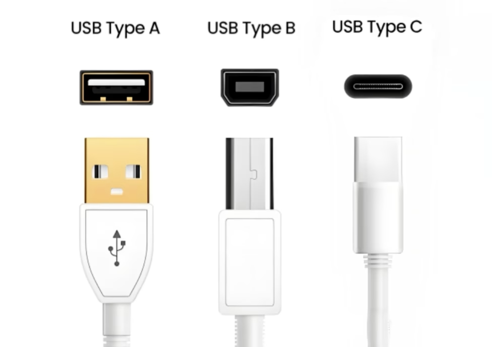
Compared to traditional USB Type-A or Type-B connectors, Type-C brings major changes:
- Physical Structure and Pins:The USB Type-C connector has 24 pins arranged in a symmetrical layout. This means the PCB layout density is much higher. The design must also handle the signal reversal mechanism. The connector is smaller, requiring precise pad design and alignment with the PCB edge.
- Electrical Capabilities:Traditional USB usually only provides 5V power. With USB PD, Type-C supports 5V, 9V, 15V, 20V, and higher voltage levels, with current up to 5A. This requires the PCB to handle high voltage and high current on power traces. It also needs proper thermal management and a dedicated PD controller chip.
- Multifunction Signals:The Type-C interface uses the Configuration Channel (CC) pins to negotiate and switch signal roles dynamically. Besides USB data, it can transmit DisplayPort, PCIe, Thunderbolt, and other high-speed protocols. This multiplexing requires designers to have a clear plan for signal routing.
1.2 Main Design Challenges
Designing a good USB Type-C PCB means solving these core challenges:
- High-Speed Signal Integrity:Handling differential signals at 10Gbps or higher. This requires strict impedance control, continuous signal return paths, and minimized crosstalk.
- High-Power Integrity:Carrying currents of several amperes. The design must ensure low DC voltage drop and effective heat dissipation.
- Complex Control Logic:Correctly handling the CC pins with pull-up and pull-down resistors. This is needed for connection detection, orientation detection, and role definition.
- EMC and ESD Protection:Placing ESD protection devices and common-mode filters correctly in a small space. They must protect the ICs without affecting the quality of high-speed signals.
2 Key Pins and Layout Strategy
2.1 Pin Groups and Functions of the Type-C Connector
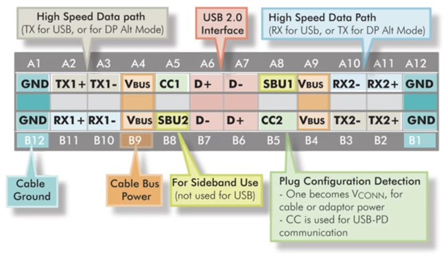
Understanding the pin functions is the first step for PCB layout. The 24 pins are grouped by function:
- Power and Ground:VBUS (4 pins) and GND (4 pins). Multiple pins are used in parallel to carry high current. The PCB layout must connect these pins to large power and ground planes or wide traces.
- High-Speed Data Lanes:SuperSpeed differential pairs. This includes two TX pairs (TX1+/-, TX2+/-) and two RX pairs (RX1+/-, RX2+/-). These are the highest speed signals and have the strictest routing rules.
- Low-Speed / Sideband Channels:CC1 and CC2 are the core control pins. They handle connection detection, orientation detection, power capability advertisement (using pull-up resistor Rp), and device role definition (using pull-down resistor Rd). SBU1 and SBU2 are for sideband signals like audio or DisplayPort.
- Legacy USB 2.0:D+ and D-. This provides backward compatibility and forms one differential pair.
2.2 Golden Rules for Component Placement
Good placement is half the battle for successful routing. Here are key placement rules based on experience:
- ConnectorPosition: Place the Type-C connector as close to the PCB edge as possible. A distance of 3-5mm from the board edge is typical. This ensures easy plugging and unplugging of the external cable.
- Position of Protection and Filtering Components:ESD protection devices and common-mode chokes (or common-mode filters) must be placed very close to the Type-C connector. This suppresses or discharges static electricity before it enters the main PCB area. The recommended order is: ESD protection device → Common-mode choke → Resistors and capacitors. All related signal lines should pass under or between these components first. The distance from the ESD device to the connector should be as short as possible, for example, less than 1.5mm.
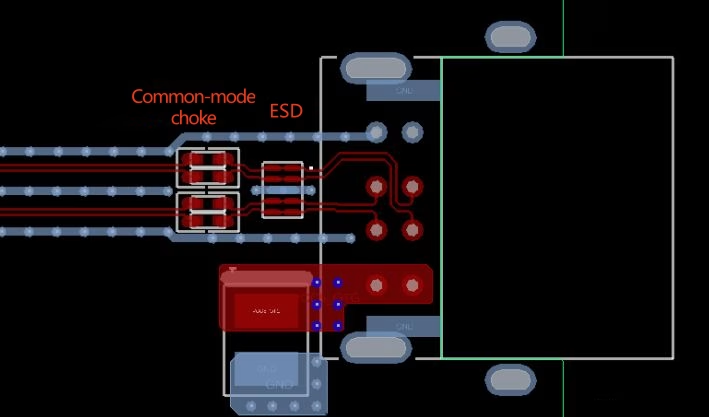
- Position of AC Coupling Capacitors:USB 3.x/4 TX and RX signals are AC coupled. The key rule is: TX signal coupling capacitors must be placed near the connector. RX signal coupling capacitors are usually provided by the other device. The local side should follow the IC datasheet. This placement helps optimize signal quality.
- Initial Power and Ground Planning:During placement, plan wide copper areas for VBUS and GND. If the design uses a protective ground (PGND), keep some distance (e.g., 2mm) between it and the system ground. Connect them at a single point using a ferrite bead or a 0-ohm resistor. Also, place enough ground vias in the PGND area to provide a low-impedance discharge path.
3 Detailed Guide to High-Speed Differential Pair Routing
The most critical part of USB Type-C design is routing the 6 differential pairs: one USB 2.0 D+/D- pair, and four SuperSpeed pairs (two TX, two RX). For signals at ≥5Gbps, routing must be very precise.
3.1 Impedance Control
All USB differential pairs must have a target impedance of 90Ω ± 10%. This requires accurate stack-up design and calculation. During routing, ensure each differential pair has a continuous and solid reference plane (usually the ground plane). Never route across a split in the reference plane, as this causes impedance changes and signal reflections.
3.2 Routing Path and Reference Plane
- Priority and Short Paths:Treat differential signals as the highest priority signals on the PCB. Keep the path as short as possible. It is recommended to keep traces shorter than 6 inches (about 15 cm) to minimize loss.
- Good Reference Plane:Each differential pair should be adjacent to at least one solid ground plane. The best case is to have ground planes on both sides (stripline structure). If routing on the outer layer (microstrip), the layer directly below (L2) must be a solid ground plane.
3.3 Length Matching
Length matching is critical for maintaining the phase relationship of differential signals and suppressing common-mode noise.
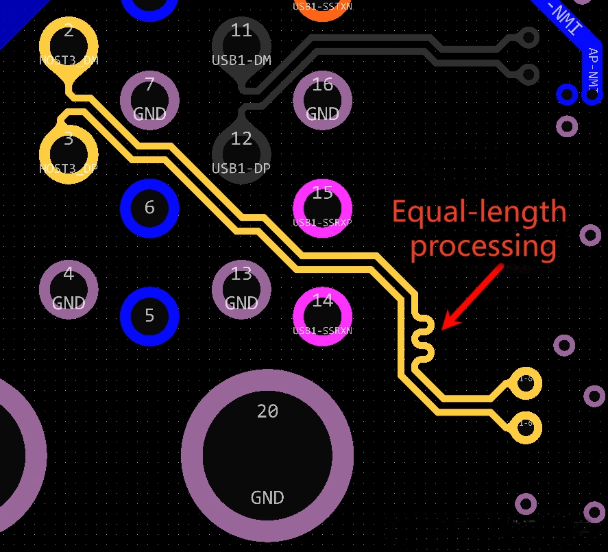
- Intra-Pair Matching:The two traces within the same differential pair (e.g., TX1+ and TX1-) must have tightly matched lengths. It is recommended to keep the length difference within ±5 mils (about 0.127mm) . Matching should be done near vias or close to the receiving end.
- Inter-Pair Matching:For high-speed signals in the same group (e.g., TX1 and TX2), matching is not as strict as intra-pair matching. However, to optimize timing, some length control is often needed. The specific tolerance should follow the main chip or protocol requirements.
3.4 Spacing Control
- Intra-Pair Spacing:The two traces in a differential pair should be closely coupled. The spacing is determined by the impedance calculation and must be consistent along the entire path.
- Pair-to-Pair and Pair-to-Other Signals Spacing:To reduce crosstalk, keep enough distance between different differential pairs, and between differential pairs and other signals. A common rule of thumb is to maintain a spacing of at least 4 times the trace width (4W) . For example, if the differential trace width is 5 mils, the spacing to other signals should be greater than 20 mils.
3.5 Vias and Layer Transitions
- Minimize Vias:Vias add parasitic capacitance and inductance that can hurt signal quality. Minimize the number of layer transitions, typically no more than 2.
- Add Return Path Ground Vias:When a differential pair must change layers, place ground vias immediately next to the signal vias. These ground vias provide a low-impedance path for the high-frequency return current. This significantly improves signal integrity and reduces EMI issues. Ideally, each differential pair transition should be paired with one ground via, or multiple surrounding ground vias.
4 Advanced Design for High-Speed (≥8Gbps) and Special Cases
When the USB Type-C interface carries signals at 8Gbps or higher (like USB 3.2 Gen2 10Gbps, USB4 20Gbps/40Gbps, or DP Alt Mode), basic rules may not be enough. More advanced techniques are needed.
4.1 Detailed Design in the Connector Area
- Center Exit:Route high-speed signals from the center of the connector pad if possible. This reduces discontinuity caused by fan-out.
- Ground Pad Treatment:For each ground pad on the connector, it is recommended to use at least two ground vias. Place these vias as close to the pad as possible to minimize ground inductance.
- Reference Plane Voiding:This is an advanced technique. It compensates for the parasitic capacitance of the connector pad. By creating a void in the reference plane (e.g., L2) directly under the connector pad, you can adjust the local impedance back to the target 90Ω. You may need to void one or two layers and reference a deeper layer. There is no standard size for these voids. The exact size and shape depend on your stack-up, materials, and connector. It must be modeled and optimized using simulation software.
4.2 Smart Routing for USB 2.0 Signals
USB 2.0 is a lower-speed differential pair. But in Type-C designs, its connection points are in the center of the connector, surrounded by high-speed and power pins. Routing space is very limited.
Broadside Coupling Technique: When it’s very hard to route the D+/D- lines out from the center pins using normal edge coupling, you can use broadside coupling. This means routing the two lines on adjacent layers (e.g., L8 and L9). They use the coupling between layers to maintain their differential characteristics. This method allows the traces to cross over or go around obstacles vertically. They can then connect to the ESD device through vias. This technique often requires HDI PCBs with blind and buried vias.
4.3 CC Pin and Power Routing
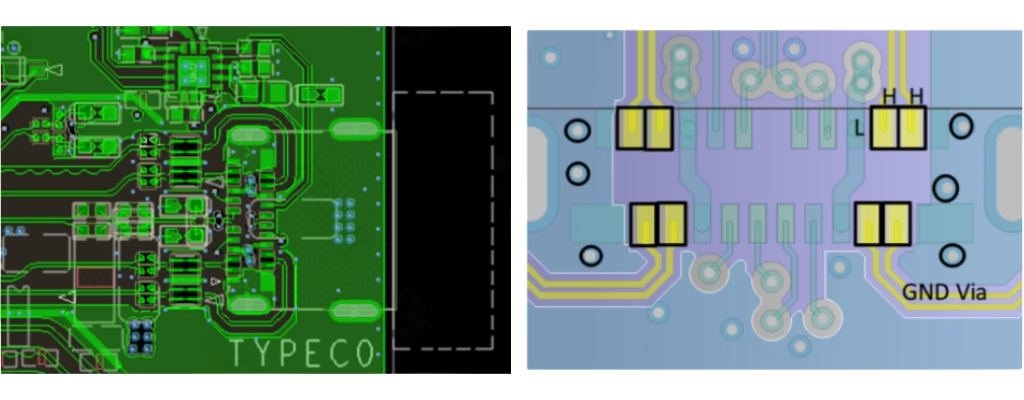
- CC Pin Routing:CC1 and CC2 are the core of Type-C logic. They need to connect to a pull-up resistor (Rp) or a pull-down resistor (Rd, typically 5.1kΩ) for power role definition. Although not high-speed, keep these traces away from high-frequency switching noise sources. If they carry PD negotiation signals, the current sense lines may need to be wider.
- VBUS/GND Power Routing:Each VBUS and GND pin must carry high current. Because the pin pitch is small, a single via often cannot handle the required current. For each power pin, use multiple vias in parallel (e.g., 3 vias) to connect to the inner layer power or ground plane. This ensures enough current capacity and helps with heat dissipation.
5 Design for Manufacturing (DFM) and Reliability
Design must not only focus on electrical performance. It must also ensure the board can be manufactured reliably. This is especially important for high-density connectors like Type-C.
5.1 Pad Design and Spacing
- Pin-to-Pin Spacing:To ensure good SMT yield and avoid solder bridges, the edge-to-edge spacing between adjacent pins should not be less than 0.2mm. This also affects the stencil design.
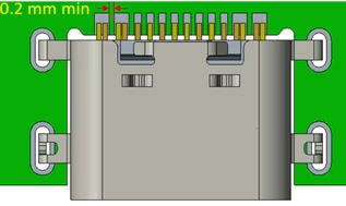
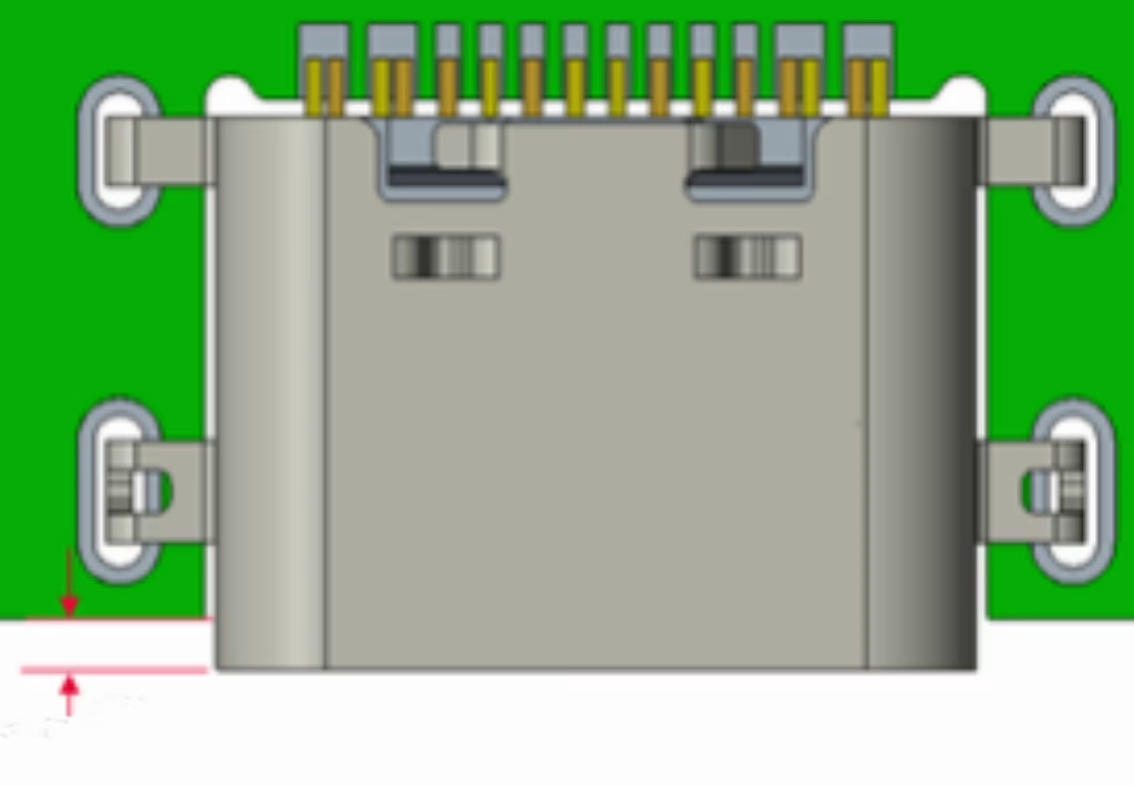
- Mounting Holes and Board Edge:Type-C connectors often have mounting posts or holes. These handle mechanical stress during plugging and unplugging. These holes are often Non-Plated Through Holes (NPTH). It is critical to follow the connector datasheet carefully. Pay attention to the keep-out area requirements around NPTHs. Because NPTHs are drilled at the very end of PCB fabrication, they have larger tolerances. They need larger clearances than plated holes. Ignoring this can lead to manufacturability issues, like pads being cut. The fit between the PCB edge and the connector front must also follow the drawing exactly.
5.2 PCB Thickness Selection
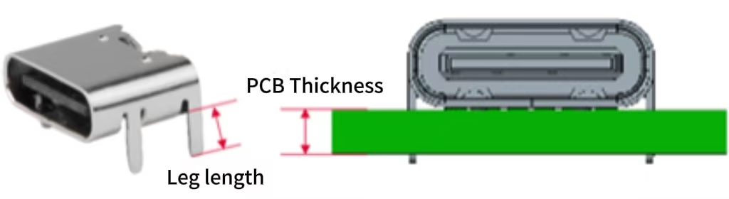
PCB thickness depends on the connector’s mounting type:
- SMD Type:There is no strict limit on PCB thickness for surface-mount connectors. Any thickness works as long as the footprint matches.
- Through-Hole Type:
Reflow Soldering: The pin length should be greater than two-thirds of the PCB thickness for reliable soldering.
Wave Soldering: The pin must extend at least 0.5mm past the bottom of the PCB.
5.3 Managing Supply Chain Challenges
In engineering practice, there can be a conflict between the component supplier’s (connector) strict requirements and the PCB manufacturer’s capabilities. When a connector’s DFM requirements (like very tight hole tolerances or complex NPTH slots) are difficult for the board house, the correct approach is to bring the connector supplier and PCB manufacturer together. Work with them to find a compromise that both sides can accept, rather than forcing one side to comply. This issue is more common in flexible PCB designs, where material tolerances are larger. More design flexibility is needed in those cases.
6 FAQs
Q1: My design only uses USB 2.0 signals but has a Type-C connector. Do I still need to control impedance to 90Ω during routing?
A1: Yes, it is still recommended to control impedance to 90Ω. Although USB 2.0 is less strict about impedance (it can usually work at 90Ω), the Type-C connector and its pin layout are designed for high-speed SuperSpeed signals. Even if you don’t use the high-speed pairs now, the unused pins and traces can become points of impedance mismatch and affect signal quality. Maintaining consistent impedance is a good practice for robust design and future compatibility.
Q2: Does the 5.1kΩ pull-down resistor on the CC pins need to be exact? Can I use a different value?
A2: You must use a 5.1kΩ resistor with 1% tolerance. The USB Type-C specification defines the standard pull-down resistance (Rd) as 5.1kΩ. This value is used by the device (Sink) to identify itself to the Source and for orientation detection. Using a wrong value can cause role detection to fail or power negotiation errors, potentially preventing charging or correct device identification.
Q3: How do I do length matching for a differential pair in a very tight space?
A3: For differential pairs, length matching should be done near vias or close to the signal receiving end. The common method is to add “accordion” or “trombone” bends to the shorter trace. However, these bends can introduce crosstalk. To minimize this, follow the “3W” rule: the spacing between the bend and any parallel section of the trace should be at least 3 times the trace width. Also, spread the matching compensation out rather than concentrating it in one spot.
Q4: Can I copy a fixed void size from a reference design for the ground plane under the connector, without doing my own simulation?
A4: This is strongly not recommended. Voiding the reference plane is a very fine-tuning technique. The optimal size depends heavily on your specific stack-up (dielectric thickness, material), pad size, and the connector’s parasitics. Copying a size that doesn’t match your design can make the impedance worse, not better. If you cannot simulate, a safer option is to keep the reference plane solid. Alternatively, strictly follow the voiding recommendations from your connector vendor’s official evaluation board or design guide, if available and validated for your stack-up.
Q5: My Type-C interface needs to handle 20V/5A power. What should I pay attention to in routing?
A5: First, the VBUS and GND traces must be wide enough for the current. You may need to use copper pours instead of thin traces, depending on the copper weight. Second, for each VBUS and GND pin, use multiple vias in parallel (e.g., 3-4 vias) to connect to the inner layer power or ground plane. This shares the current and helps with heat dissipation. Third, maintain enough creepage distance between high-voltage and low-voltage areas to prevent arcing. Finally, consider adding a temperature sense line or work with the PD controller for accurate current monitoring.
Q6: What is a Dual-Role Port (DRP)? Are there special design requirements?
A6: A Dual-Role Port (DRP) is a port that can act as either a Source (like a charger) or a Sink (like a phone). An example is a laptop that can be charged or charge another device. The design challenge is that the CC pin circuit must dynamically switch between Rp (pull-up) and Rd (pull-down). This usually requires a dedicated USB Type-C controller chip that supports the DRP function. The hardware design must provide the correct connections and configuration for this controller.
7 Conclusion
Designing a PCB for a USB Type-C interface is a complex engineering task. It combines challenges from high-speed digital design, RF design (signal integrity), high-power analog design, and precision mechanical design. Every step is critical, from choosing the connector and stack-up, to routing differential pairs and vias, to the final DFM check.
Summary of key success factors:
- Placement First:Strictly follow the placement order for components, especially protection devices and coupling capacitors.
- Impedance is Key:Always base high-speed signal routing on 90Ω impedance control and solid reference planes.
- Details Matter:Strictly match intra-pair lengths, add return path vias correctly, and handle power pin current capacity well.
- Close the Loop with Manufacturing:Consider DFM from the start. Communicate with your supply chain to ensure the design can be turned into a reliable product.
As data rates continue to increase, designing for USB Type-C will become even more challenging. Continuous learning, using professional simulation tools, and following industry best practices are the keys to creating excellent products. We hope this guide helps you avoid common mistakes and design USB Type-C products that are high-performance, stable, and reliable.
OrinewPCB has focused as a one-stop PCB assembly manufacturer from PCB Manufacturing to Electronic Components Sourcing to PCB Assembly to Test to Program IC for more than 14 Years with reliable quality and fastest delivery for global clients.