
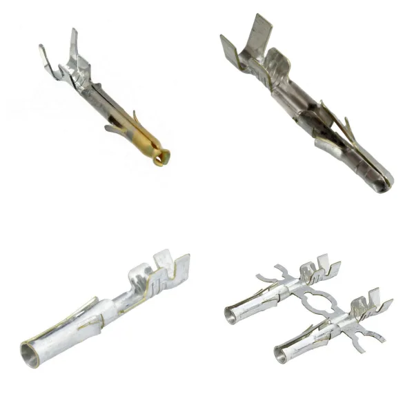
<h1> Multi Purpose </h1> <p> Products in the multipurpose contact family are interconnect system components which are typically applied to a conductor by means of a crimp connection, which can be used with multiple styles of corresponding housings. This allows the use of the same contact part number and application equipment to assemble similar connectors which are resistant to incorrect mating. </p> <p>
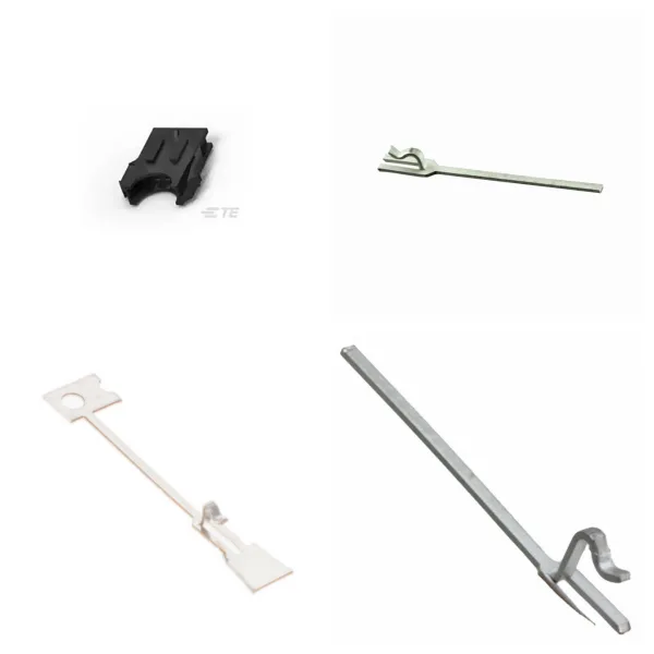
<h1> Leadframe </h1> <p> Leadframe is one of the core components of semiconductor packaging, mainly used to support the chip and establish its electrical connection with the external circuit. </p> <p>   </p> <h2> 1. Leadframe Overview </h2> <h3> 1) ‌Core Composition‌ </h3> <p> <strong>‌Die Paddle‌</strong>: Provide mechanical support for the chip to ensure the stability of the chip during the packaging process. </p> <p> <strong>‌Lead Finger‌</strong>: Divided into inner pins (connected to the chip pad through bonding wires) and outer pins (connected to the PCB board) to achieve electrical signal transmission. </p> <p>   </p> <h3> 2) ‌Main Function‌ </h3> <p> <strong>‌Mechanical Support‌</strong>: Fix the chip and prevent the molding compound from overflowing. </p> <p> <strong>‌Electrical Connection‌</strong>: Bridge the chip and the external circuit through bonding wires (gold, aluminum, copper wire). </p> <p> <strong>‌Heat Dissipation Path‌</strong>: Use the thermal conductivity of metal materials to transfer chip heat. </p> <p>   </p> <h2> 2. What is the Manufacturing Process of Leadframe? </h2> <p> <strong>‌Stamping Method</strong>‌ </p> <p> High-speed stamping of metal strips through precision molds is suitable for low-density packaging with a pin count of <100, with low cost but limited precision. </p> <p>   </p> <p> <strong>‌Etching Method</strong>‌ </p> <p> Use photolithography and chemical etching (such as FeCl₃) to form high-precision graphics, suitable for high-density packaging (such as QFN), low equipment cost but high material consumption. </p> <p>   </p> <h2> 3. What are the Material Properties of Leadframe? </h2> <h3> 1) ‌Common Alloys‌ </h3> <p> ‌Copper-based Alloys‌ (such as Cu-Fe-P, Cu-Ni-Si): conductivity>80% IACS, strength>450MPa, taking into account both conductivity and mechanical strength. </p> <p>   </p> <p> ‌Iron-nickel Alloys‌ (such as Alloy 42): The thermal expansion coefficient is close to that of silicon (4.8-5.2ppm/℃), reducing package cracking caused by thermal stress. </p> <p>   </p> <h3> 2) ‌Performance Requirements‌ </h3> <p> Must meet tensile strength, electrical/thermal conductivity, softening temperature resistance (>500℃), and etching/stamping processability. </p> <p>   </p> <h2> 4. Development Trend of Leadframe </h2> <p> <strong>‌High Density‌</strong>: The pin pitch is reduced from 1.27mm to 0.15mm, supporting higher integration packaging. </p> <p> <strong>‌Pinless‌</strong>: QFN and DFN packages replace traditional exposed pin designs to increase PCB layout density. </p> <p> <strong>‌Material Innovation‌</strong>: Develop high-strength and high-conductivity copper alloys (such as tensile strength > 600MPa and conductivity > 80% IACS) to meet ultra-thin requirements. </p> <p>   </p> <h2> 5. What is Leadframe Used for? </h2> <p> Mainly covers consumer electronics, automotive electronics, and industrial control fields, suitable for low- and medium-complexity chip packaging with I/O count < 300. </p> <p> ‌Consumer Electronics‌: such as QFP and SOP packages in mobile phones and home appliances; </p> <p>   </p> <p> <strong>‌Automotive Electronics‌</strong>: TO packages for power devices and DFN packages for sensors; </p> <p> <strong>‌Industrial Control‌</strong>: DIP, PLCC, and other scenarios with high reliability requirements. </p> <p>   </p> <h2> 6. Leadframe FAQs </h2> <h3> 1) What are the common failure modes of Leadframe? ‌ </h3> <p> <strong>‌Delamination‌</strong>: Interface separation due to mismatch of material thermal expansion coefficient (CET); </p> <p> <strong>‌Pin Oxidation‌</strong>: Copper alloys are easily oxidized and require surface coating protection; </p> <p> ‌Mechanical Fatigue‌: Pin bending or package stress causes fracture. </p> <p>   </p> <h3> ‌2) What is the difference between Lead Frame and substrate packaging (such as BGA)? ‌ </h3> <p> <strong>‌Structure‌</strong>: Lead Frame is a single-layer metal frame, and substrate packaging uses a multi-layer wiring substrate; </p> <p> <strong>‌I/O Density‌</strong>: Lead Frame is suitable for medium and low density (300 pins); </p> <p> <strong>‌Cost‌</strong>: Lead Frame has a lower cost, and substrate packaging has high complexity. </p>
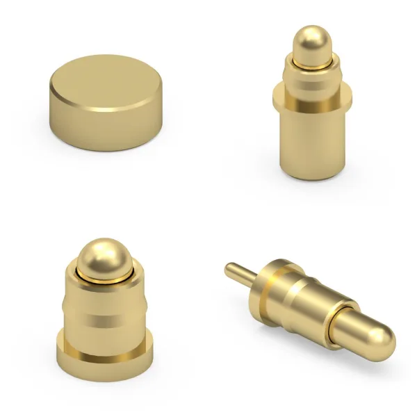
<h1> Contacts, Spring Loaded (Pogo Pins), and Pressure </h1> <p> Spring-loaded contacts, also known as "pogo pins" in reference to the toy they resemble, are commonly used to establish electrical contact between two objects whose relative mechanical position cannot be well-controlled, or a connector system tolerant of frequent mating/unmating cycles is desirable. Charging cradles for cordless handheld devices such as bar code scanners and mobile radios are a common example. Contact pads used to create a durable, corrosion-resistant surface for spring-loaded contacts to bear against are also included within this product family. </p> <p>

Contacts

‌Contacts‌ in electronic components are the core components of connectors, which are mainly responsible for realizing the conduction function of electrical connection and are indispensable basic components in modern electronic devices.


1. What is the ‌Basic Structure of Contacts?‌

1) ‌Material Composition‌: Contacts are usually made of highly conductive metal materials, such as copper alloys, gold/silver plating, etc., to ensure low resistance and high reliability.

2) ‌Morphological Design‌: According to different application scenarios, contacts can be divided into:

‌Terminal‌: Fixed end for wire crimping or welding.

‌Pin‌: Active end that cooperates with the socket to form a pluggable connection.


2. What are the ‌Functional Characteristics of Contacts?‌

‌Signal Transmission‌: Conducting circuits through physical contact to transmit electrical signals or electrical energy.

‌Current Carrying‌: Need to meet specific current capacity requirements, commonly seen in power interfaces or high-power device connections.


3. What are the ‌Technical Key Points of Contacts?‌

Plating Process‌: Surface plating (such as gold plating, and nickel plating) can improve corrosion resistance and contact stability.


‌Elastic Design‌: Some contacts adopt a reed structure to ensure contact pressure and durability during plugging and unplugging.


4. What are the Types of Contacts?‌

Type

Typical Application Scenarios

Features

Power Terminal

Power adapter, industrial equipment power supply interface

High current carrying, high-temperature resistance

Signal Pin

Data cable, PCB board connector

High-frequency signal transmission, low impedance requirements

Elastic Contact Piece

SIM card slot, battery contact

Miniaturization, high plug-in life


5. What is the Failure Mode of Contacts?

Oxidation/Contamination: Oxidation of the contact surface or adhesion of foreign matter leads to increased resistance.


Mechanical Fatigue: Frequent plugging and unplugging causes deformation or breakage of elastic elements.


6. What are Contacts Used for?

Widely used in consumer electronics (such as mobile phones and computers), automotive electronics, industrial control equipment and communication base stations.
