Why Choose the Halogen-Free PCB?

Table of Content
As the electronics industry moves toward greener and more sustainable development, material selection is no longer just a trade-off between cost and performance. It now involves corporate responsibility, global regulations, and product safety throughout its entire life cycle. As the core component of electronic products, the environmental attributes of printed circuit boards (PCBs) have drawn increasing attention. Among the various eco-friendly options, halogen-free PCBs have quickly become a mainstream choice because they offer clear advantages in safety, reliability, and electrical performance.
This article explains what halogen-free PCBs are, their material systems, key properties, manufacturing challenges, typical applications, and future trends. It aims to help engineers and decision-makers understand why choosing halogen-free PCBs is not only a technically sound decision but also a forward-looking strategy.
1. Halogen and PCBs: Why the Shift?
1.1 Role of Halogen in Electronics
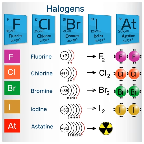
Halogens are the five elements in Group 17 of the periodic table: fluorine, chlorine, bromine, iodine, and astatine. In the electronics industry, chlorine and bromine are the most commonly used. Halogens are added to traditional PCBs for two main reasons:
- Flame retardancy: Brominated flame retardants (such as TBBPA) are added to epoxy resins to help PCBs meet the UL94 V-0 flammability rating. When exposed to fire, these compounds release bromine radicals that interrupt the combustion reaction, slowing or stopping the flame.
- Process aid: Chlorinated solvents were once widely used for cleaning and etching PCBs, though they have been gradually phased out.
1.2 Environmental and Health Concerns
Halogens are relatively stable during the useful life of a PCB. The main problems arise when products are discarded and incinerated. Burning halogen-containing PCBs can produce dioxins and furans, which are persistent organic pollutants. These substances are:
- Highly toxic: Dioxins are classified by the World Health Organization as known human carcinogens. Even at very low levels, they can harm the immune and endocrine systems.
- Bioaccumulative: These compounds do not break down easily and build up in the food chain, eventually affecting ecosystems.
In addition, burning halogenated materials releases corrosive gases such as hydrogen chloride (HCl) and hydrogen bromide (HBr), which can harm rescue workers and damage equipment during fires.
For these reasons, while the EU RoHS directive does not ban all halogens, the International Electrotechnical Commission (IEC) and major electronics brands have introduced stricter halogen-free standards. These standards are driving the industry toward greener materials.
2. Definition and Standards for Halogen-Free PCBs
2.1 What Is a Halogen-Free PCB?
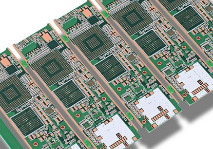
A halogen-free PCB does not mean that no halogens are present. Instead, it means that no halogen-containing substances are intentionally added to any part of the PCB—including the base material, solder mask, and legend ink—and any residual halogen content is kept below strict industry limits.
2.2 Key Standards and Limits
The two most widely accepted standards for halogen-free PCBs are:
| Standard | Chlorine (Cl) Limit | Bromine (Br) Limit | Total Halogen Limit |
| IPC-4101B | ≤ 0.09% (900 ppm) | ≤ 0.09% (900 ppm) | ≤ 0.15% (1500 ppm) |
| IEC 61249-2-21 | ≤ 0.09% (900 ppm) | ≤ 0.09% (900 ppm) | ≤ 0.15% (1500 ppm) |
A PCB that meets either of these standards can be called halogen-free. In practice, certification usually requires a test report from a third-party lab such as SGS or CTI, and sometimes the UL “Halogen-Free” mark on the UL yellow card.
3. Material Systems and Properties of Halogen-Free PCBs
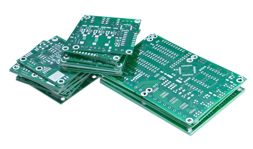
3.1 Halogen-Free Flame Retardant Mechanisms
Traditional brominated flame retardants work mainly in the gas phase, interrupting the combustion chain reaction. Halogen-free materials use condensed-phase mechanisms. Common approaches include:
- Phosphorus-based: Phosphorus-containing compounds (such as DOPO) are incorporated into the epoxy resin. When heated, they promote the formation of a dense char layeron the material surface. This layer blocks oxygen and heat while reducing smoke.
- Nitrogen-based: Compounds like melamine release non-flammable gases when decomposed, diluting combustible gases.
- Inorganic metal hydroxides: Aluminum hydroxide (ATH) and magnesium hydroxide (MDH) absorb large amounts of heat and release water vapor when decomposing. They provide both flame retardancy and smoke suppression.
3.2 Halogen-Free Laminate Materials
Halogen-free copper-clad laminates (CCL) are made by bonding halogen-free epoxy resin with glass fabric. Typical material parameters are shown below:
| Material Type | Tg (DSC, °C) | Td (5%, °C) | CTE-z (ppm/°C) | T260 (min) | T288 (min) |
| Standard Halogen-Free FR-4 | 140-150 | 360-380 | 40-45 | ≥60 | ≥30 |
| High-Tg Halogen-Free FR-4 | 170-180 | 360-380 | 35-40 | ≥60 | ≥15-30 |
| High-Frequency Halogen-Free | 150-200 | 350-400 | 30-40 | ≥60 | ≥30 |
Key Parameter Explanations:
- Tg (Glass Transition Temperature): Indicates the temperature resistance of the material. High-Tg materials (≥170°C) are suitable for lead-free soldering and automotive electronics.
- Td (Decomposition Temperature): Shows thermal stability. A higher Td means the material is less likely to decompose or delaminate during soldering.
- CTE-z (Z-axis Coefficient of Thermal Expansion): Affects via reliability. Lower CTE-z means less thermal stress between layers and longer plated-through hole life.
3.3 Electrical Properties of Halogen-Free Materials
Compared to traditional FR-4, halogen-free materials have distinct electrical characteristics:
- Dielectric Constant (Dk) and Dissipation Factor (Df): Specially designed halogen-free high-frequency materials can achieve Df as low as 0.005–0.008 (at 1 GHz), close to PTFE. This makes them suitable for 5G communication and high-speed digital signals.
- Comparative Tracking Index (CTI): Halogen-free materials typically have a CTI ≥ 600V (PLC 0), which is much better than traditional brominated materials (usually PLC 2–3). This provides better resistance to tracking failure in high-voltage, high-humidity environments.
4. Key Benefits of Halogen-Free PCBs
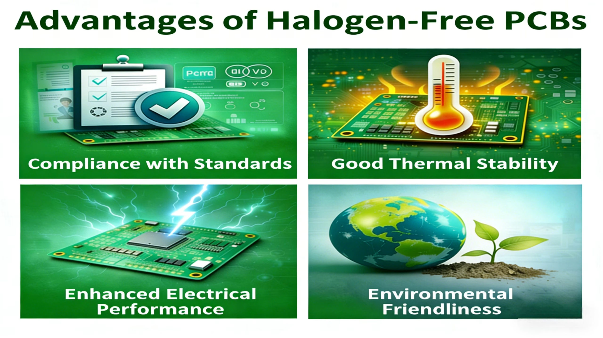
4.1 Environmental and Health Benefits
This is the fundamental reason for using halogen-free PCBs. Choosing halogen-free materials means:
- No dioxin formation: No persistent organic pollutants are generated when products are incinerated at end of life. This aligns with circular economy principles.
- Safer factory environment: Reducing exposure to halogen-based chemicals during manufacturing protects workers.
- Green supply chain compliance: Major electronics brands (such as Apple, Dell, and Huawei) require halogen-free materials. Using them is essential for entering these supply chains.
4.2 Improved Reliability and Safety
Halogen-free materials often outperform traditional materials in key reliability areas:
- Better heat resistance: Higher Tg and Td mean better resistance to delamination and blistering during lead-free reflow soldering (peak temperatures 245–260°C).
- Lower CAF risk: Conductive anodic filament (CAF) is a common failure mode in PCBs. Halogen-free materials have lower ionic contamination, which significantly reduces CAF risk.
- Higher CTI: Suitable for high-voltage applications such as power supplies and electric vehicles.
4.3 Electrical Performance Advantages
For high-frequency and high-speed applications, the low dissipation factor of halogen-free materials offers:
- Better signal integrity: Lower signal loss and delay, suitable for high-speed digital interfaces operating above 10 Gbps.
- More stable impedance control: Dk varies less with temperature and humidity, helping maintain consistent characteristic impedance.
4.4 Regulatory Compliance and Market Access
Globally, halogen-free regulations and standards are becoming stricter:
- EU: While RoHS does not ban all halogens, REACH restricts certain brominated flame retardants.
- China: The “Administration Method for the Restriction of Hazardous Substances in Electrical and Electronic Products” encourages green design.
- Japan: JIS C 0950 (J-Moss) controls specific hazardous substances.
Using halogen-free PCBs helps companies meet regulatory requirements and improve their competitiveness in international markets.
5. Manufacturing Challenges and Process Control
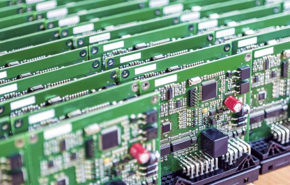
Halogen-free materials have unique physical and chemical properties that require careful process control during PCB fabrication.
5.1 Drilling
Halogen-free materials often contain hard fillers such as aluminum hydroxide or phosphorus-based additives, making them harder than traditional FR-4. As a result:
- Drill bit wear is faster: Drill life is typically reduced by 30–50%.
- Hole wall quality is critical: Feed rate and spindle speed must be optimized to prevent burrs or rough hole walls.
5.2 Desmear
Halogen-free resin systems are more chemically resistant. The conventional potassium permanganate desmear process may not effectively remove smear from hole walls. Therefore:
- Desmear parameters (chemical concentration and treatment time) must be adjusted for the specific material.
- For high-reliability applications, plasma treatmentcan be used to achieve a cleaner hole wall surface and better copper adhesion.
5.3 Lamination
Halogen-free materials generally absorb more moisture than traditional FR-4. If stored improperly or not baked before lamination, residual moisture can vaporize during high-temperature lamination, causing:
- Lamination voids
- Delamination
Thus, manufacturers must follow strict pre-baking procedures (e.g., 120°C for 4–8 hours) and optimize the lamination temperature profile.
5.4 Soldering Compatibility
Halogen-free PCBs generally perform well in lead-free reflow soldering due to their higher Tg and Td. However, attention is still needed to:
- Control the ramp rate to avoid excessive thermal shock.
- Keep peak temperature around 245°C ± 5°C to prevent material degradation.
6. Typical Applications of Halogen-Free PCBs
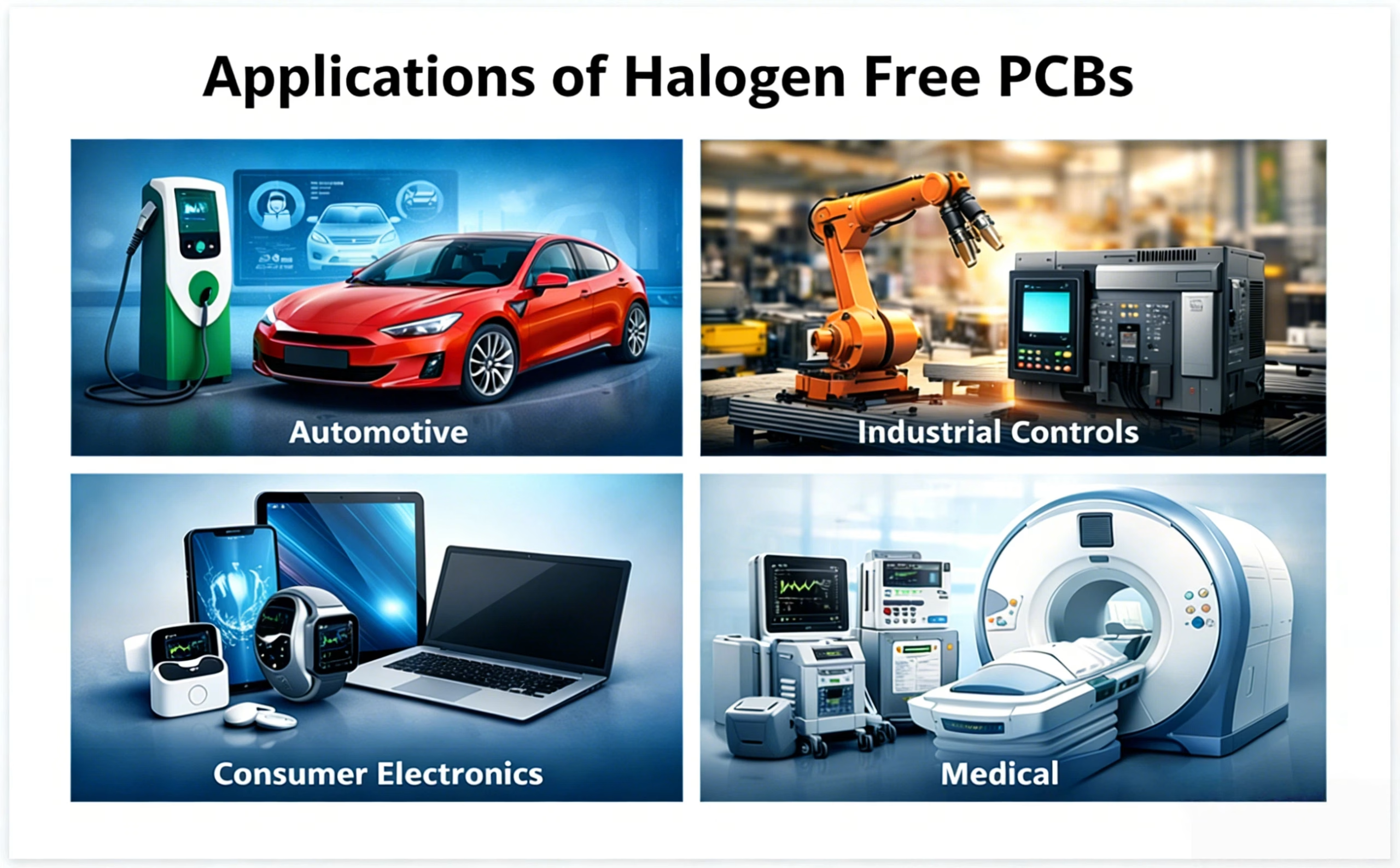
As material performance improves and costs decrease, halogen-free PCBs are used in many industries.
(1)Consumer Electronics
Smartphones, tablets, laptops, and wearables. These products have short life cycles and high recycling pressure. Halogen-free materials are now a standard requirement from major brands. Common uses include motherboards, battery connectors, and display modules.
(2)Automotive Electronics
The shift to electric and connected vehicles demands high reliability. Halogen-free PCBs are used in:
Powertrain: Engine control units (ECU), battery management systems (BMS)
ADAS: Radar/camera modules, domain controllers
In-vehicle communication: Infotainment systems, telematics boxes
High-Tg halogen-free materials (Tg ≥ 170°C) are widely adopted in automotive applications.
(3)Communication Equipment
5G base stations, optical modules, core network equipment, and high-end servers. These applications require low dissipation factor and excellent signal integrity, making low-Df halogen-free high-frequency materials an ideal choice.
(4)Industrial and Medical
Industrial controls, precision instruments, and medical devices. The high insulation reliability (high CTI) and low ionic contamination of halogen-free materials make them well suited for high-voltage, high-humidity, and high-cleanliness environments.
(5)Other High-End Applications
Aerospace, military electronics, and LED lighting (high-thermal-conductivity halogen-free metal-core PCBs) are also increasingly adopting halogen-free solutions to meet both environmental and reliability requirements.
7. FAQs
(1) Do halogen-free PCBs contain no halogens at all?
No. Halogen-free means halogen content is kept below strict limits (Cl and Br each ≤ 900 ppm). It does not mean zero halogens. A more accurate term is “low halogen” or “no intentionally added halogen.”
(2) How much more do halogen-free PCBs cost compared to traditional PCBs?
Typically, halogen-free PCBs cost 10–30% more than traditional FR-4 of the same specifications. The cost difference comes from higher raw material prices, faster drill bit wear, and more complex process control. However, the gap is shrinking as technology improves and volumes increase.
(3) Can halogen-free PCBs be used in high-frequency or high-speed designs?
Yes, but the material must be specifically designed for that purpose. Not all halogen-free laminates have low dissipation factor. For applications above 10 Gbps or in microwave bands, it is important to check the Dk and Df values and their stability with frequency.
(4) How can I verify that a PCB is halogen-free?
Reliable methods include: 1) Asking for a test report from an accredited third-party lab (e.g., SGS, CTI); 2) Checking the UL yellow card for the “Halogen-Free” or “HF” mark; 3) Working with PCB manufacturers that have a strong material traceability system.
(5) Are there special storage or handling requirements for halogen-free PCBs?
Yes. Because halogen-free materials are more moisture-absorbent, they are usually shipped in vacuum-sealed bags. Once opened, they should be processed within 24 hours. If exposed to ambient conditions longer, pre-baking (120°C for 4–6 hours) is recommended to remove absorbed moisture and prevent delamination.
8. Summary
The rise of halogen-free PCBs reflects a broader shift in the electronics industry—from focusing solely on performance to balancing performance, environmental responsibility, safety, and sustainability. This is not just a simple material replacement. Through phosphorus-based, nitrogen-based, and other new flame retardant systems, halogen-free technology combines good flame retardancy, high reliability, strong electrical performance, and environmental friendliness.
For engineers, choosing halogen-free PCBs helps ensure regulatory compliance, reliability, and long-term value from the start of a project. For companies, adopting halogen-free technology is a strategic move to participate in global green supply chains, fulfill corporate responsibility, and build brand resilience.
Today, halogen-free PCBs are already widely used in consumer electronics, automotive, and communication equipment. As material science advances and costs continue to decline, their applications will expand further. It is clear that in the future of electronics, a “green” PCB will be an important indicator of product quality and corporate responsibility.
OrinewPCB has focused as a one-stop PCB assembly manufacturer from PCB Manufacturing to Electronic Components Sourcing to PCB Assembly to Test to Program IC for more than 14 Years with reliable quality and fastest delivery for global clients.
Related Posts
ORINEWPCB · PROJECT SUPPORT
Contact Us
Discuss your PCB assembly project with our team.
FREE QUOTE
Plan your turnkey PCBA build.
Share your quantity and requirements. Add Gerber files and a BOM when ready.
Files are optional for an initial discussion. Include any assembly, sourcing or testing requirements in your message.