USB Type-C PCB Design: Layout, Routing & Assembly Checklist

Table of Content
- 1. Define the USB-C port before choosing the footprint
- 2. Review CC1, CC2 and the circuit roles
- 3. Set layout and routing constraints from the real interface
- 4. Review ESD protection, VBUS and the shield separately
- 5. Verify connector fit and assembly before releasing boards
- 6. Define acceptance tests for both plug orientations
- 7. Prepare the USB-C turnkey PCBA RFQ package
- 8. USB Type-C PCB design FAQ
USB TYPE-C PCB DESIGN · LAYOUT, ROUTING & BUILD RELEASE
Quick answer: A reliable USB-C PCB starts with a defined data interface, power role and exact connector. Check CC termination and orientation handling, use the selected connector’s land pattern, agree the stack-up and routing constraints with the PCB manufacturer, and plan ESD protection and the VBUS path. Before assembly, release matching Gerber, BOM and placement files and specify tests in both plug orientations. A Type-C receptacle alone does not establish USB speed, Power Delivery capability or product compliance.
This guide answers a practical question: what should an engineer check before releasing a USB-C board for fabrication and assembly? The answer differs for a USB 2.0 device, a SuperSpeed interface and a USB Power Delivery product. Treat these as deliberate requirements rather than assuming every Type-C connector needs the same circuit or routing rules.
For a build-ready design, request an OrinewPCB turnkey PCBA and BOM review. Include the actual connector part number, board revision and required port functions so sourcing, fabrication and assembly can be reviewed together.
1. Define the USB-C port before choosing the footprint
USB Type-C describes the connector system. The implemented USB data protocol and power behavior are separate decisions. A product may use a Type-C receptacle for USB 2.0 and a 5 V power input without implementing SuperSpeed or higher-voltage Power Delivery. Conversely, adding a PD controller does not by itself add a faster USB data interface.
Write down the data role, power role, supported modes and intended cable before placement starts. Power source/sink and data host/device are different classifications; do not assume they always move together. A dual-role design needs the controller behavior and power path appropriate to its actual requirements.
| Application | Decisions to release | Avoid this assumption |
|---|---|---|
| USB 2.0 device with Type-C input | Device PHY and speed, sink behavior, CC implementation, VBUS sensing/protection and connector pinout. | Every Type-C board needs SuperSpeed routing or a PD controller. |
| SuperSpeed / USB4 interface | Actual protocol and lane configuration, orientation routing, PHY/mux choices and channel constraints. | A USB 2.0-only receptacle or an arbitrary mux supports the intended interface. |
| Power Delivery product | Supported power profiles, source/sink roles, controller configuration, cable capability and complete power path. | A connector current rating permits any requested voltage or power automatically. |
| Alternate-mode product | Negotiation, permitted pin assignments, switching and the supported system/cable combination. | All alternate modes are enabled by fitting the receptacle. |
2. Review CC1, CC2 and the circuit roles
CC1 and CC2 participate in attachment and orientation detection. The termination must match the port’s power role. For a receptacle-based sink using discrete Rd terminations, CC1 and CC2 need independent pull-down paths; do not short them together and use one shared resistor. A common nominal Rd is 5.1 kΩ, but the applicable specification and chosen controller determine the implementation and permitted tolerance. Some controllers integrate the termination.
A source presents Rp behavior; a dual-role port manages the appropriate role behavior. Copying a sink resistor circuit into a source design is not a valid shortcut. Check the controller’s unpowered or dead-battery behavior if the product must start from an external supply.
- Mark the exact controller and connector MPNs and check their pin numbering and drawing views.
- Identify which functions are implemented by the controller and which need external parts.
- Review CC protection and any short-to-VBUS exposure against actual device ratings.
- For USB 2.0, connect the receptacle’s corresponding D+ contacts to the D+ network and corresponding D− contacts to the D− network as required by the connector implementation. Review the escape geometry and minimize unnecessary branches.
- For higher-speed lanes, release the orientation/mux connection scheme rather than assuming all TX/RX contacts can simply be tied together.
Do not add USB 3.x-style AC coupling capacitors to USB 2.0 D+/D−. For interfaces that do require AC coupling, use the relevant PHY and system guidance for values, existing integrated coupling and placement. The same capacitor rule does not apply to every pin carrying a USB-related signal.
3. Set layout and routing constraints from the real interface
Begin the layout review with the selected PHY’s current hardware guidance and the fabricator’s proposed stack-up. A trace-width number copied from another board does not establish the impedance of yours: copper geometry, dielectric thickness and material all matter. Our controlled-impedance PCB service is relevant when the fabrication requirements call for defined impedance and associated verification.
| Routing decision | Engineering review | Fabrication / review evidence |
|---|---|---|
| Impedance | Specify the required target and tolerance for each implemented interface; USB 2.0 high-speed designs commonly use a 90 Ω differential target. | Approved layer stack, material assumptions, trace geometry and any required coupon/report. |
| Reference path | Keep a continuous return reference; review splits, voids and transitions before accepting a route. | Layer views showing the reference copper throughout the route. |
| Pair matching | Distinguish skew within a pair from requirements between different pairs. Use the actual PHY/channel limits. | Constraint report with units, endpoints and any package-delay assumptions. |
| Vias and stubs | Review transitions, asymmetry, return connections and unused branches against the channel requirements. | Via structure and stub review; any special fabrication process explicitly agreed. |
| Protection and optional filtering | Check the selected device’s loading and package routing; justify a choke or filter rather than adding it by habit. | Exact MPN, layout recommendation and channel assessment. |
There is no universal “six-inch maximum,” fixed via count or single length-matching tolerance for every USB-C product. A short connection can still fail if its topology is wrong; an arbitrary matching meander can also worsen a layout. Use the limits for the implemented PHY, connector and channel, then document how the released design meets them.
Do not copy a reference-plane void from a different connector or stack-up. Any deliberate impedance compensation around pads needs a defined geometry and suitable validation. Likewise, assigning the two members of a pair to separate layers is a distinct transmission-line structure, not a routine escape workaround that preserves the original routing calculation automatically.
4. Review ESD protection, VBUS and the shield separately
Make the protection path deliberate
Place appropriate protection near the exposed connector and review the route from the connector through the protection to the protected circuit. Long branches to a TVS or an inductive return can undermine the protection. Match device capacitance, working voltage and clamping behavior to the actual protected signal and component.
Agree the shield/chassis connection as part of the product’s EMC and mechanical design. Do not apply a universal split-ground distance or copy a ferrite/zero-ohm link without checking the reference design’s purpose and your own enclosure. Component selection and layout are inputs to validation; they do not establish an ESD compliance result by themselves.
Size the complete power path
Review the connector contacts, protection, switching devices, copper, vias and return path for the intended operating conditions. Document the permitted voltage, current, temperature rise and voltage drop. Do not turn a generic example such as “three vias per power pin” into a production requirement without calculation and review.
If USB PD is used, confirm the controller configuration, intended power profiles and the relevant cable requirements. The manufacturing test must distinguish “power appeared” from successful negotiation and the specified load behavior. The requested product power and temperature conditions belong in the build specification, not only in an email saying “USB-C charging.”
5. Verify connector fit and assembly before releasing boards
Use the exact connector drawing and land-pattern revision. “USB-C socket” is not a sufficient purchasing description. Top-mount, mid-mount and other receptacle constructions can differ in board fit, shell features and contact layout. A package that looks similar is not automatically footprint-compatible.
Check board thickness, board-edge position, enclosure opening, mating access, terminal geometry, locating features and shield tabs together. Surface-mount contacts do not remove the need to check board thickness and mechanical constraints. Identify each hole or slot as plated or non-plated from the approved drawing; do not assume every mounting feature is NPTH.
- Footprint: confirm drawing view, pad numbering, mask/paste openings, mounting features and copper restrictions.
- Mechanical fit: check the connector against the board profile and enclosure model, including tolerances and intended assembly sequence.
- Soldering: agree the process for signal contacts and shell features, using the component’s permitted process conditions.
- Inspection: establish how accessible and obscured joints will be assessed; X-ray is considered where applicable rather than assumed to reveal every possible defect.
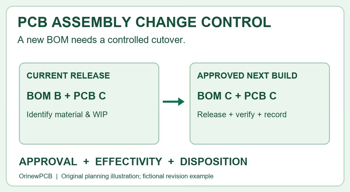
- Substitutions: require engineering approval of mechanical, electrical and process compatibility before purchasing a replacement MPN.
For sourcing, browse OrinewPCB connector options or send the approved MPN in the BOM. Availability, price, source and lead time are confirmed for the actual requirement; a catalog listing is not a live inventory promise. A sourcing change that affects the connector can require a footprint or enclosure review before assembly.
6. Define acceptance tests for both plug orientations
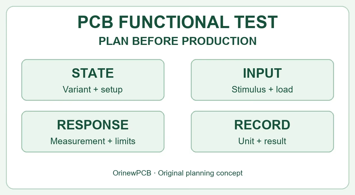
Assembly inspection and a power LED are not complete proof of port functionality. Release a test procedure that identifies the hardware and firmware revisions, test equipment and cables, expected behavior and acceptance limits. Repeat the relevant connection and operating checks with the plug reversed; include the product’s required host/device and power combinations.
| Evidence | Example check to define | What it does not prove alone |
|---|---|---|
| Assembly inspection | Connector position, orientation, contacts and shell attachment against agreed criteria. | USB enumeration, protocol behavior or high-speed compliance. |
| Power behavior | Attach/detach, expected supply behavior and agreed load condition; PD negotiation when implemented. | All data modes or operating combinations. |
| Data function | Enumeration and the required communication check with specified host, firmware and cable, in both orientations. | Every host/cable combination or signal-quality margin. |
| Product validation | Any required electrical, mechanical, EMC/ESD or USB compliance evaluation under a defined procedure. | A guarantee derived from AOI, flying probe or connector appearance. |
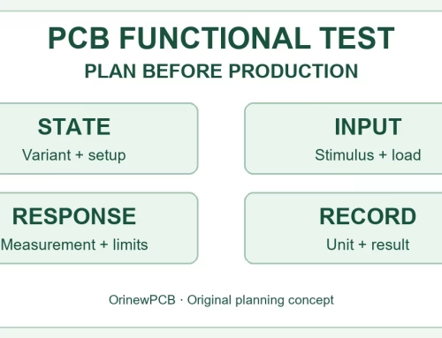
For the test handoff, identify who supplies fixtures, software, approved cables and limit values. Define what is recorded for each unit and what happens after a failure or rework. Our PCBA functional test plan checklist explains how to turn a functional requirement into repeatable production acceptance steps.
Example: a USB 2.0-only sensor board
Illustrative planning example, not a customer project: a team releases revision B of a sensor board with a Type-C receptacle, a USB 2.0 device interface and a 5 V sink input. The RFQ identifies the exact connector and the CC implementation, supplies a common revision for Gerber/BOM/placement files, and defines enumeration plus a sensor-data exchange on an approved host in both orientations. It explicitly excludes SuperSpeed, PD higher-voltage operation and alternate modes.
This description lets the assembler review the intended build and test scope without inferring features from the connector’s shape. The team still owns the approved design and acceptance limits; a manufacturing review does not replace interface validation or certification.
7. Prepare the USB-C turnkey PCBA RFQ package
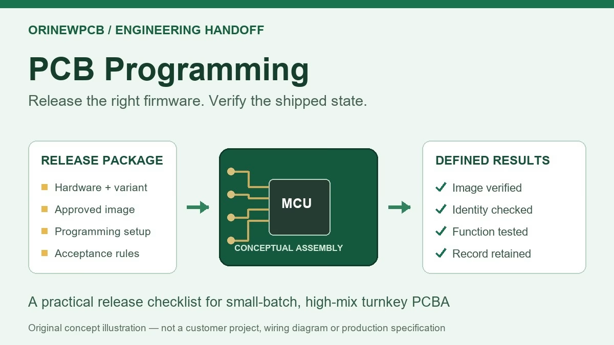
For small and medium batches or multiple board variants, identify which connector, controller configuration and firmware belong to each revision. Keep alternatives and do-not-populate items explicit. A useful package contains:
- PCB release: Gerber/drill files, board outline, material and stack-up notes, plus required impedance details.
- Assembly release: BOM with exact MPNs and manufacturer names, placement file, assembly drawing and connector orientation/fit notes.
- Sourcing scope: full turnkey or clearly identified customer-supplied parts; approved alternatives and packaging requirements.
- Port requirements: data interface, power/data roles, implemented modes and controller/firmware versions.
- Acceptance scope: inspection criteria, orientation-aware functional checks, fixtures/cables, records and any separate compliance work.
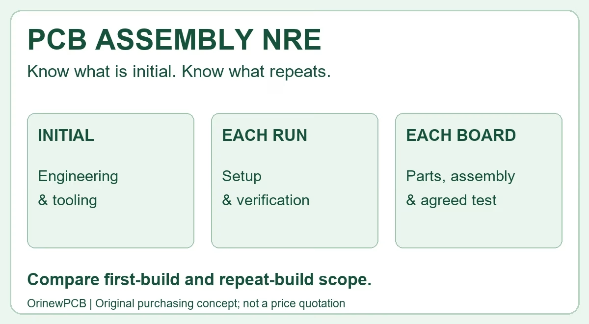
- Commercial inputs: quantity by variant, repeat-order expectations, requested destination and target date. The achievable schedule follows material and process review.
Bring the design, BOM and assembly plan together. OrinewPCB provides PCB fabrication, component sourcing and turnkey PCB assembly, with particular focus on small/medium batches and high-mix builds. We use new, original electronic components and coordinate the agreed inspection and test scope. Our nine-stage quality workflow does not mean every board receives nine identical functional tests or automatic USB compliance certification.
Send the files you have, your quantities and the required USB-C functions. Ask for a coordinated review of connector sourcing, PCB requirements, assembly access and production testing before committing to the build.
Request a USB-C Turnkey PCBA & BOM Review
Need to clarify responsibilities first? See our turnkey PCB assembly service scope.
8. USB Type-C PCB design FAQ
Does a USB-C connector mean the board supports USB4 or Power Delivery?
No. The receptacle does not determine the implemented data rate, power role, PD features or alternate modes. Check the circuit, controller, firmware and supported cable/system combination.
Can a USB 2.0 device use a Type-C receptacle?
Yes, with the appropriate USB 2.0 connections, CC behavior, power handling and connector implementation. A USB 2.0-only design does not acquire SuperSpeed capability by changing the connector.
Can CC1 and CC2 share one sink pull-down resistor?
For a receptacle-based sink using discrete Rd terminations, provide independent termination paths. Check whether the controller already integrates them and use its approved implementation. Do not short CC1 and CC2 together.
What trace width and length-matching tolerance should I use?
Use the selected interface/PHY constraints and the actual fabricated stack-up. A universal width, spacing, length or via count is not a substitute for a defined impedance and channel review.
Can I substitute a similar-looking Type-C connector?
Only after engineering approval. Compare the exact pinout, land pattern, shell/mounting features, board fit, ratings, mating interface and assembly requirements. Update the BOM and affected drawings consistently.
Does bare-board electrical testing prove that the USB-C port works?
No. Bare-board electrical tests concern PCB connectivity. Assembly inspection and agreed powered functional tests address different coverage. USB protocol, signal integrity and compliance requirements need their own appropriate validation.
Technical guidance is application-dependent. Use the current interface specifications and the exact connector, PHY, controller and protection-device documentation for the released product. Original concept figures and the example above are explanatory material, not manufacturing dimensions or a certified reference design.
Related Posts
ORINEWPCB · PROJECT SUPPORT
Contact Us
Discuss your PCB assembly project with our team.
FREE QUOTE
Plan your turnkey PCBA build.
Share your quantity and requirements. Add Gerber files and a BOM when ready.
Files are optional for an initial discussion. Include any assembly, sourcing or testing requirements in your message.