
PCB Soldering: How To Achieve Perfect PCB Soldering

Table of Content
In the intricate world of electronics, Printed Circuit Boards (PCBs) serve as the backbone, connecting countless components to create functional devices. At the heart of this connectivity lies soldering—a fundamental process that forms robust electrical and mechanical links between components and the PCB’s conductive traces. Far from being a mere technical task, perfect PCB soldering is an art that demands precision, practice, and a deep understanding of its principles. A well-executed solder joint ensures optimal circuit performance, reliability, and longevity, while a poor one can lead to frustrating failures and hours of troubleshooting.
Whether you’re a hobbyist assembling a DIY project, a student learning electronics, or a professional engineer, mastering soldering techniques is an indispensable skill. This comprehensive guide will demystify the soldering process, covering everything from basic definitions and essential tools to advanced techniques and common pitfalls. Our aim is to equip you with the knowledge and confidence to achieve perfect PCB soldering every time.
1. What Exactly is PCB Soldering?
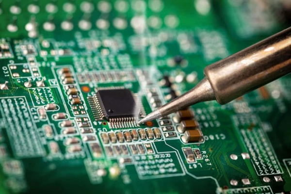
At its core, soldering is a metallurgical process where two or more metal items are joined together by melting and flowing a filler metal (solder) into the joint. The solder, having a lower melting point than the base metals, flows into the gap between the components and the PCB pad. Upon cooling, it solidifies, creating a strong electrical and mechanical bond without melting the components or the PCB traces themselves. This process is distinct from welding, where the base metals are melted directly.
The primary purpose of soldering on a PCB is two-fold:
- Electrical Connection:To establish a reliable pathway for current flow between a component and the circuit board.
- Mechanical Connection:To physically secure components to the board, ensuring they remain in place even under vibration or stress.
Solder typically consists of a metal alloy, traditionally a tin-lead (Sn-Pb) mixture, but increasingly lead-free alternatives (e.g., tin-silver-copper or Sn-Ag-Cu) are used due to environmental regulations. The choice of solder impacts melting temperature, flow characteristics, and joint reliability, making it a critical consideration for any soldering project.
2. Unveiling the Different Types of PCB Soldering
While the fundamental principle of joining metals with solder remains the same, the methods employed vary significantly based on scale, component type, and production volume . Here are the primary types of soldering used in PCB manufacturing:
2.1 Manual (Hand) Soldering
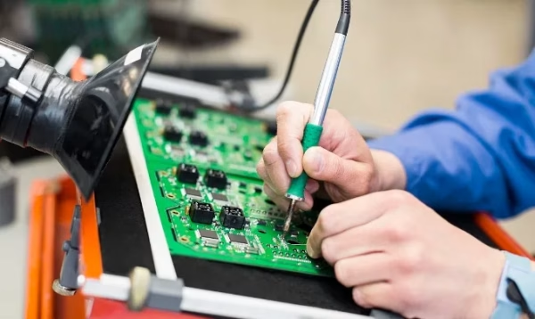
This is the most common method for prototyping, repairs, and low-volume production. It involves an operator using a soldering iron to manually heat a joint and apply solder. It requires skill, precision, and a steady hand but offers flexibility and immediate control over the process. Ideal for through-hole components (THC) and some surface-mount devices ( SMD) when rework is needed.
2.2Wave Soldering
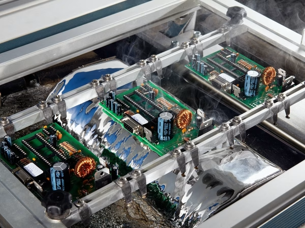
Primarily used for high-volume production of through-hole component boards. In this automated process, PCBs with components already inserted pass over a wave of molten solder. The solder adheres to the component leads and pads, forming all joints simultaneously. It’s efficient for large batches but less suitable for complex boards with a mix of THCs and SMDs due to potential overheating of smaller components.
2.3Reflow Soldering
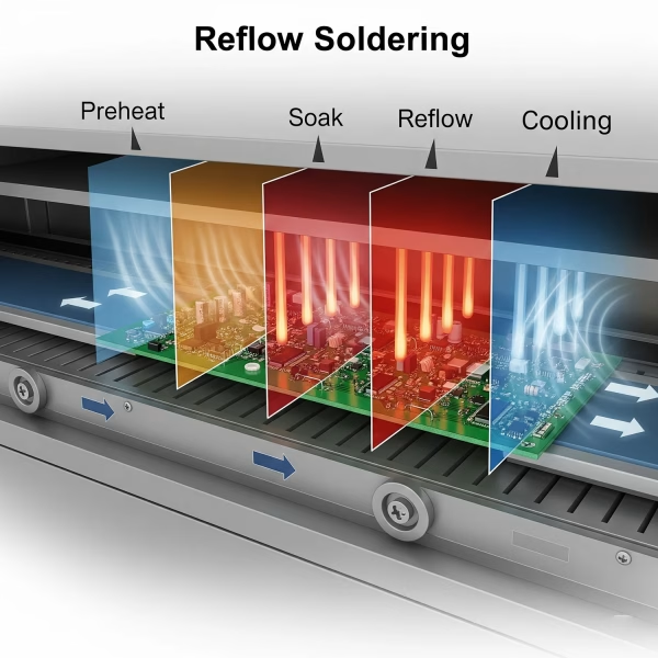
The standard method for soldering Surface-Mount Devices (SMDs). Solder paste—a mixture of powdered solder and flux—is first applied to the PCB pads using a stencil. Components are then placed onto the sticky paste. The entire assembly is then moved through a reflow oven, which heats the board in carefully controlled zones. The solder paste melts (reflows), coalesces around the component leads, and then cools to form solid joints. This method is highly precise and suitable for high-density boards.
2.4 Selective Soldering
A specialized automated process often used for boards with a combination of SMDs and through-hole components. It’s an alternative to wave soldering for through-hole parts when the board also contains heat-sensitive SMDs on the bottom side that might be damaged by a full wave pass. A precisely controlled nozzle delivers a small, localized wave of molten solder to specific through -hole joints, protecting surrounding components.
3. Essential Tools and Materials for Successful Soldering
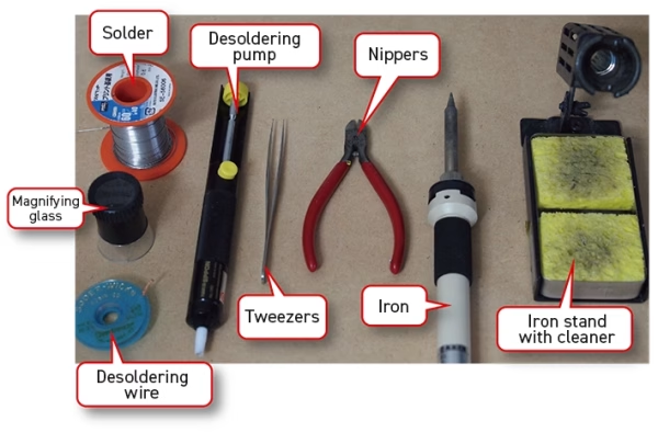
Having the right tools and materials is crucial for achieving high-quality solder joints. Here’s a rundown of what you’ll need, especially for manual soldering:
| Tool/Material | Description | Purpose |
| Soldering Iron/Station | Comes in various watt ages; a temperature-controlled station is ideal. Different tips are available (chisel, conical, hoof). | Heats the joint to melt solder. Temperature control prevents damage to components and PCB. |
| Solder Wire | A metallic alloy (e.g., Sn60/Pb40, Sn63/Pb37, Sn96.5/Ag3/Cu0.5). Typically has a flux core. | The filler metal that forms the electrical and mechanical bond. |
| Flux | A chemical cleaning agent, often found in the solder core or as a separate liquid/gel. | Cleans oxidation from component leads and PCB pads, allowing solder to flow smoothly (wetting). |
| Desoldering Pump (Solder Sucker) | A spring-loaded vacuum tool. | Removes excess molten solder from a joint . |
| Desoldering Braid (Solder Wick) | Braided copper wire impregnated with flux. | Wicks away molten solder through capillary action, effective for fine pitch components or clearing holes . |
| Safety Glasses | Protects eyes from splashing solder or flux fumes. | Essential eye protection. |
| Fume Extractor/Fan | A fan with a carbon filter. | Removes harmful solder fumes from your breathing zone. |
| Heat-Resistant Mat | Protects your workbench from heat and solder splashes. | Workspace protection. |
| Helping Hand/PCB Holder | A stand with adjustable arms and clips. | Holds the PCB and components steady, freeing your hands. |
| Wire Cutters/Flush Cutters | Small , sharp pliers. | Trims excess component leads after soldering. |
| Tweezers | Fine-tipped, non-magnetic. | Handles small components and wires with precision. |
| Isopropyl Alcohol (IPA) & Cotton Swabs/Brush | Cleaning solution. | Removes flux residue after soldering for a clean finish. |
| Multimeter | Measures voltage, current , resistance, and continuity. | Tests solder joints for continuity and shorts. |
4. Your Step-by-Step Guide: How to Solder a PCB Manually
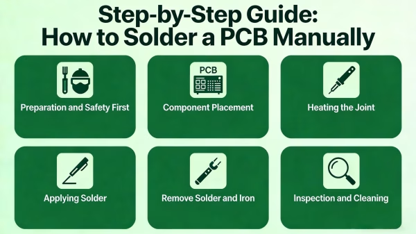
Achieving a perfect solder joint involves a precise sequence of actions. Follow these steps for reliable manual soldering:
4.1 Preparation and Safety First
- Cleanliness:Ensure your PCB, component leads, and soldering iron tip are perfectly clean. Use IPA if necessary.
- Ventilation:Set up your fume extractor or work in a well-ventilated area to avoid inhaling harmful fumes.
- Safety Gear:Put on your safety glasses.
- Organize:Arrange your tools and components within easy reach. Use a helping hand to secure the PCB.
- Tin the Tip:If your soldering iron tip is new or not shiny, apply a small amount of solder to it. This “tins” the tip, improving heat transfer and preventing oxidation.
4.2 Component Placement
- Insert the component into its designated holes on the PCB.
- For through-hole components, bend the leads slightly on the underside of the board to hold them in place. This prevents them from falling out when you flip the board to solder.
4.3 Heating the Joint
- Position the soldering iron tip so that it simultaneously touches both the component lead and the surrounding PCB pad. This ensures even heat distribution to both surfaces.
- Hold the iron steady for 2-3 seconds, allowing the heat to transfer and bring both the lead and the pad up to the solder’s melting temperature.
4.4 Applying Solder
- While the iron is still heating the joint, feed a small amount of solder wire directly onto the heated joint—not onto the iron tip itself. The solder should melt and flow smoothly, surrounding the component lead and covering the pad, forming a shiny, conical fillet.
- Apply just enough solder to create a strong connection without creating a blob or bridge.
4.5 Remove Solder and Iron
- First , remove the solder wire from the joint.
- Immediately after, lift the soldering iron tip away from the joint.
- Allow the joint to cool naturally and solidify. Do not blow on it or move the component, as this can create a “cold joint.”
4.6 Inspection and Cleaning
- Visual Inspection:Examine the joint. A good solder joint should be shiny, smooth, concave (like a tiny volcano or fillet), and fully cover both the lead and the pad.
- Trim Leads:Use flush cutters to trim any excess component leads close to the solder joint.
- Clean Residue:Use IPA and a cotton swab or brush to clean off any remaining flux residue, which can be corrosive or unsightly.
5. Common Soldering Mistakes to Avoid
Even experienced solderers can make mistakes. Recognizing and correcting these common errors is key to improving your skills:
| Mistake | Description/Appearance | Impact | How to Avoid/Fix |
| Cold Joint | Dull, lumpy, grainy, or “cracked” appearance. Solder didn’t flow properly. | Poor electrical connection, intermittent signals, mechanical weakness. | Ensure sufficient heat (iron tip on lead and pad simultaneously) and proper tinning. Allow joint to cool undisturbed. |
| Solder Bridge | Solder accidentally connects two adjacent pads, traces, or component leads. | Causes a short circuit, preventing the circuit from functioning or potentially damaging components. | Use minimal solder. Be precise with solder placement. If detected, remove excess solder with wick or pump. |
| Overheating/Lifted Pad | Too much heat applied for too long. Can cause the copper pad to delaminate from the PCB or damage heat-sensitive components. | Permanent PCB damage, component failure. | Use a temperature-controlled iron. Heat for only 2-3 seconds before applying solder. Use appropriate tip size for heat transfer. |
| Insufficient Solder | The joint looks “hungry” or sparse; doesn’t fully cover the pad or secure the lead. | Weak electrical connection, fragile mechanical bond. | Apply enough solder to form a proper fillet. Ensure good wetting by pre-tinning the lead if needed. |
| Excessive Solder | A large, rounded blob of solder that obscures the component lead and pad. | Can mask a cold joint underneath, wastes solder, increases risk of bridging. | Practice feeding only the necessary amount of solder. If excess, remove with wick/pump and re-solder. |
| Dry Joint / Not Enough Flux | Similar to a cold joint, but caused by insufficient flux, leading to oxidation preventing proper wetting. | Poor flow, dull joint, weak connection. | Use solder with a good flux core or apply external flux if needed, especially for older components. Ensure surfaces are clean. |
| Moved Component While Cooling | The component or lead was bumped or moved before the solder fully solidified. | Can create a fractured or cold joint. | Keep components perfectly still for a few seconds after removing the iron. |
6. Expert Tips for Flawless PCB Soldering
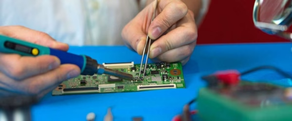
Beyond avoiding common mistakes, incorporating these best practices will elevate your soldering game:
- Maintain a Clean Tip:Always keep your soldering iron tip clean by wiping it on a damp sponge or brass wool before and after each joint. Re-tin the tip with a tiny bit of fresh solder periodically to prevent oxidation and ensure efficient heat transfer.
- Choose the Right Tip:Use a tip size appropriate for the component and pad size. A larger tip transfers heat more efficiently to larger pads/leads, while a fine tip is essential for intricate SMD work.
- Temperature Control is Key:If you have a temperature-controlled soldering station, set the temperature correctly for your solder type (e.g ., 300-350°C for lead-free, 280-320°C for leaded) and component sensitivity. Adjust as needed; too low won’t melt the solder, too high can damage components/PCB.
- Pre-Tinning Leads:For stubborn or oxidized component leads, apply a small amount of solder to the lead before inserting it into the PCB. This “pre-tinning” improves solder flow and connection.
- Flux is Your Friend:Don’t underestimate the power of flux. If your solder isn’t flowing well, or if you’re working with old components, applying a dab of extra flux (liquid or gel) can significantly improve wetting and joint quality.
- Practice the “Two-Second Rule”:Most through-hole joints should be completed within 2-5 seconds. Too little heat results in a cold joint ; too much causes overheating. Develop a rhythm.
- Patience and Observation:Take your time. Observe how the solder melts and flows. It should look like mercury flowing around the joint. If it balls up, something isn’t hot enough or clean enough.
- Invest in Good Lighting and Magnification:A well-lit workspace and a magnifier (like a jeweler’s loupe or a bench magnifier) are invaluable for inspecting joints and spotting defects, especially with smaller components.
- Regular Maintenance:Clean your workspace, regularly replace worn-out iron tips, and ensure your desoldering tools are in good working order.
- Start Simple:If you’re new to soldering, begin with simple kits or practice boards that use large through-hole components. Gradually move on to more complex projects.
7. FAQs
Leaded solder (e.g., Sn60/Pb40, Sn63/Pb37) contains lead, melts at a lower temperature, and flows very well, often producing shinier joints. Lead-free solder (e.g., Sn96.5/Ag3/Cu0. 5) is environmentally friendlier, requires higher temperatures, and can be slightly harder to work with, sometimes resulting in duller-looking joints, though still electrically sound.
If the solder melts instantly and flows smoothly onto the joint, the temperature is likely good. If it takes too long to melt, the temperature is too low. If the solder smokes excessively , burns quickly, or the tip oxidizes rapidly, it might be too high. A temperature-controlled station is recommended for consistency.
No, plumbing solder typically has a much larger diameter and often contains different flux types that can be corrosive to electronics. Always use rosin-core solder specifically designed for electronics.
A perfect solder joint should be shiny (for leaded solder, lead-free can be slightly duller), smooth, and have a concave shape (like a miniature volcano or fillet) that fully covers the component lead and the PCB pad. There should be no sharp points, dullness, cracks, or excessive solder.
Apply the soldering iron to the joint to melt the solder. Immediately use a desoldering pump to suck the molten solder away, or place desoldering braid over the joint and heat the braid with the iron until it wicks away the solder. Repeat if necessary until the lead is free.
8. Summary
Mastering PCB soldering requires the right tools, precise technique, and practice. Key steps include proper preparation, simultaneous heating of pad and lead, correct solder application, and careful joint inspection. Avoid common errors like cold joints and bridging for reliable, long-lasting electronic assemblies.Making this foundational practice the cornerstone of all reliable electronics work.
OrinewPCB has focused as a one-stop PCB assembly manufacturer from PCB Manufacturing to Electronic Components Sourcing to PCB Assembly to Test to Program IC for more than 14 Years with reliable quality and fastest delivery for global clients.








