PCB Enclosure Design Guide: From Concept to Manufacturing

Table of Content
- 1. Core Design Requirements for PCB Enclosures
- 2. Material Selection: Balancing Performance, Cost, and Environment
- 3. Structural Mechanical Design for PCB Enclosures
- 4. PCB Enclosure Design Process: Two Main Methods
- 5. Off-the-Shelf Enclosures vs. Custom Enclosures
- 6. Thermal Management and EMC Design
- 7. Design for Manufacturing and Assembly (DFM/A) Guide
- 8. Common Design Mistake Checklist
- 9. Safety Compliance and Standards
- 10. Future Trends: Collaborative Design and Digital Iteration
- 11.FAQs
- 12. Summary
In electronic product development, PCB (Printed Circuit Board) design often gets a lot of attention, while enclosure design is frequently underestimated. Even if the PCB functions perfectly, poor enclosure design can still cause overheating, assembly interference, insufficient waterproofing, cable stress, or outdoor reliability test failures.
A well-thought-out enclosure is not just a “protective shell” for the product. It is a key part of thermal management, structural reliability, electromagnetic compatibility, manufacturability, and user experience. This guide will systematically explain the core requirements, material selection, structural design, manufacturing limitations, safety standards, and common mistakes of PCB enclosure design. It will help engineers and technicians avoid pitfalls and successfully bring products from concept to market.
1. Core Design Requirements for PCB Enclosures
1.1 What is a PCB Enclosure?

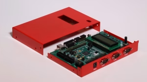
A PCB enclosure is a structural part used to house and protect a finished circuit board. It allows the circuit board to be put into use, secures the PCB, and protects it from environmental factors such as dust, moisture, and impact. At the same time, the enclosure also determines the product’s final appearance, user interaction method, and ease of installation.
The first step in enclosure design is not CAD modeling. It is to clearly define the “application scenario + protection level + functional requirements” to avoid unnecessary rework later in development.
1.2 Protection Ratings: IP and NEMA Standards
Protection ratings determine the enclosure’s material, structure, and manufacturing process. Indoor and outdoor applications require different protection standards. IP (Ingress Protection) and NEMA (National Electrical Manufacturers Association) are the two most widely used systems.
NEMA Standards (mainly for North American industrial environments):
- NEMA 1: Basic indoor protection against light dust and accidental contact. Commonly used for indoor control equipment.
- NEMA 3: Outdoor protection against dust, rain, snow, and ice formation.
- NEMA 4 / 4X: Industrial waterproof protection. The 4X rating adds corrosion resistance, suitable for coastal or chemical environments.
- NEMA 12: Enhanced indoor dust and moisture protection for industrial equipment.
IP Ratings (IEC 60529 standard, internationally used):
- IP54: Limited dust protection and splash water protection.
- IP65: Completely dustproof (level 6) and resistant to low-pressure water jets (level 5).
- IP67: Completely dustproof and can be temporarily immersed in 1 meter deep water (level 7). Suitable for harsh outdoor environments.
In industrial applications, designers should also consider safety compliance standards such as UL 50/508A, as well as IEC 61439 requirements for mechanical strength and thermal performance.
1.3 Mechanical Definition of Functional Requirements
Before starting enclosure design, the following key functional requirements must be clearly defined:
- Internal Components: PCB dimensions, mounting hole locations, connector layout, and heat-generating components that need thermal structures.
- Environmental Conditions: Indoor or outdoor use, operating temperature range, humidity, corrosion exposure, and required dust protection level.
- Assembly and Maintenance: Frequency of opening the enclosure, mounting method (wall-mounted, handheld, desktop), and cable management requirements.
- Manufacturing Process: Injection molding for mass production, or 3D printing or CNC machining for prototyping. The manufacturing method directly affects wall thickness and tolerance design.
2. Material Selection: Balancing Performance, Cost, and Environment
Material selection directly affects protection performance, durability, thermal behavior, and manufacturing cost. Common enclosure materials are mainly divided into plastics and metals.
2.1 Plastic Enclosures: Cost-Effective for Indoor Applications
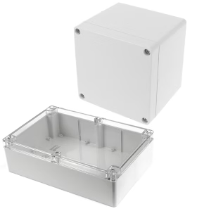
Plastic enclosures are lightweight, easy to mold, and cost-effective. They are suitable for NEMA 1 or NEMA 12 rated applications.
- ABS: Balanced mechanical properties and chemical resistance. Widely used in consumer electronics. However, long-term UV exposure can cause aging outdoors.
- Polycarbonate (PC): High impact resistance, heat resistance, and UV stability. Suitable for both indoor and outdoor applications.
- PC+ABS Blend: Improved impact resistance and low-temperature performance. Used for high-end indoor devices.
- ASA/PC Blend: Excellent weather resistance, thermal stability, and chemical resistance. Suitable for outdoor use without additional coating.
2.2 Metal Enclosures: Preferred for Industrial and Outdoor Equipment
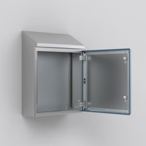
Metal enclosures provide excellent strength, corrosion resistance, and thermal conductivity. They are ideal for NEMA 3/4/4X rated applications.
- Aluminum Alloy: Lightweight and corrosion-resistant. Often anodized for improved durability. Common grades include 5052 for sheet metal and 6061 for CNC machining.
- Stainless Steel: High strength and excellent corrosion resistance. Suitable for humid or chemically aggressive environments.
- Cold-Rolled Steel: Low cost and good rigidity. Suitable for indoor applications with powder coating.
- Galvanized Steel: Zinc-coated low-carbon steel. Better moisture resistance than standard cold-rolled steel.
For 3D printed enclosure prototypes, material selection directly affects strength, heat resistance, and durability. PLA is suitable for quick validation, while ABS, PETG, and Nylon are often preferred for functional prototypes or mechanical structural parts.
3. Structural Mechanical Design for PCB Enclosures
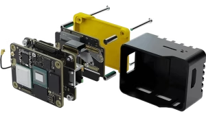
Structural design directly affects manufacturing yield, assembly reliability, and long-term durability. Key focus areas include wall thickness, tolerances, reinforcement structures, and assembly methods.
3.1 Wall Thickness Design
Uneven wall thickness can cause sink marks in injection molding or cracking in 3D printing.
- Uniform Wall Thickness: Plastic injection-molded enclosures typically use 1.5–2.5 mm wall thickness, while metal enclosures commonly use 1.0–2.0 mm. Excessively thick walls may cause sink marks and uneven cooling. Overly thin walls reduce structural rigidity and increase warpage risk.
- 3D Printing Requirements: For FDM printing, the minimum wall thickness is generally ≥0.8 mm, or at least twice the nozzle diameter.
- Fillet Treatment: Adding fillets above 0.1 mm reduces stress concentration and improves mold flow and print quality.
3.2 Clearance and Tolerance Design
Manufacturing tolerances and thermal expansion require sufficient clearance between components and enclosure structures.
- PCB-to-Wall Clearance: Maintain at least 0.5 mm spacing to avoid assembly interference.
- Connector Openings: Circular openings should be 0.2–0.3 mm larger than the connector diameter. Rectangular openings should reserve about 1 mm clearance per side.
- Snap Fits and Hinges: Moving structures generally require 0.5–1 mm clearance to prevent sticking or looseness.
3.3 Reinforcement Structures: Ribs, Gussets, and Bosses
Thin-wall structures require reinforcement to improve stiffness and durability.
- Ribs: Internal reinforcement ribs should be about 1/2 to 2/3 of the wall thickness to reduce deformation.
- Gussets: Triangular support structures that distribute stress at corners and large flat surfaces.
- Bosses: Screw bosses should be reinforced with ribs to prevent cracking during assembly. Plastic screw holes are typically designed about 0.3 mm smaller than the screw diameter for proper thread engagement.
For 3D printed enclosure prototypes, thread and joint design greatly affect assembly reliability. Compared with directly printed threads, heat-set inserts provide better durability and torque resistance, especially for repeated assembly. Proper snap-fit and boss design can also reduce cracking and improve structural strength.
3.4 Assembly and Maintenance Design
The enclosure structure should balance structural stability and ease of repair.
- Fastening Methods: Screw fastening is preferred for mass production. Snap fits or adhesives may be suitable for prototypes.
- Cable Management: Cable entry points should include strain relief or protective sleeves to prevent cable damage.
- Thermal Management: Heat-generating devices may require ventilation slots, fan mounting locations, or heatsinks, while maintaining the required IP protection level.
4. PCB Enclosure Design Process: Two Main Methods
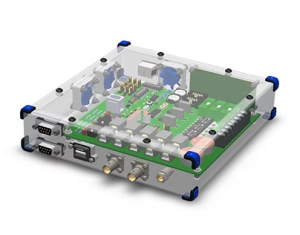
In actual development, there are two main methods for the design sequence of PCB and enclosure: the electrical-first method and the mechanical-first method. Understanding the differences helps teams collaborate more efficiently.
4.1 Electrical-First Method (Waterfall)
In the electrical-first method, the PCB size and layout are determined first. After completion, the mechanical engineer designs the enclosure around the PCB.
- Advantages: Electrical designers have full freedom to select components and place them. The design process is simple and direct.
- Disadvantages: When the product requires unique aesthetics or complex mechanical structures, there may be high interference risk or need for repeated modification later. This method often results in conservative enclosure design that becomes “box-like” just to fit the PCB.
4.2 Mechanical-First Method (Collaborative)
The mechanical-first method is suitable for products with special requirements for user experience and form factor. The design team first defines key mechanical constraints in MCAD software, such as overall PCB size, keep-out areas (including height restrictions), mounting hole locations, connector positioning, and cable paths.
- Advantages: Ensures PCB design meets enclosure requirements from the start. Reduces later rework. Particularly suitable for multi-board systems or custom-shaped enclosures.
- Disadvantages: Requires frequent communication and iteration between electrical and mechanical engineers. Demands higher team collaboration.
- Best Practice: Use cloud platforms like Altium 365 to achieve ECAD/MCAD collaboration. The mechanical engineer exports the enclosure as a STEP file and imports it into PCB design software. The electrical engineer checks component-to-enclosure interference in real-time in 3D. Alternatively, export the PCB layout as a STEP file for the mechanical engineer to design the enclosure precisely.
5. Off-the-Shelf Enclosures vs. Custom Enclosures
5.1 Off-the-Shelf Enclosures
There are many off-the-shelf PCB enclosures with standard sizes and functions available on the market. They are very suitable for prototyping or small to medium batch production.
- Advantages: Low cost, fast delivery, existing 3D models available for reference. Many off-the-shelf enclosures also have high protection ratings (such as IP67). When used with compatible panel-mount connectors, they can quickly build high-reliability systems.
- Disadvantages: Fixed size and shape may limit PCB layout or product differentiation.
5.2 Custom Enclosures
When a product requires special dimensions, complex curved surfaces, strict thermal or electromagnetic shielding requirements, custom enclosure design is necessary.
- Advantages: Perfectly fits the PCB layout. Supports branded design. High functional integration.
- Disadvantages: Long development cycle. Requires mold investment (injection molding) or higher machining cost (CNC). High risk cost of design errors.
6. Thermal Management and EMC Design
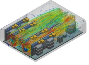
6.1 Thermal Management Strategies
- Natural Convection: Open ventilation holes at the top and bottom of the enclosure to allow hot air to rise and create airflow. Note that hole locations must avoid water paths to maintain IP rating.
- Conduction Cooling: Use a metal enclosure (especially aluminum) as a heatsink to conduct heat from the PCB to the enclosure surface. Add thermal pads or thermal grease between heat-generating components and the enclosure.
- Forced Air Cooling: For high-power devices, reserve fan mounting locations and air intake/exhaust openings.
- Local Heat Dissipation: Design cooling fins on the enclosure to increase heat dissipation area.
6.2 Electromagnetic Compatibility (EMC) and Shielding
- Metal Enclosures: Naturally provide electromagnetic shielding. However, ensure seams are electrically continuous. Gaps should not become EMI leakage paths. Grounding design is key to shielding effectiveness.
- Plastic Enclosures: Do not have shielding capability. The inside needs conductive coating, metal foil, or a metal shielding cover. For products with wireless communication (Wi-Fi, Bluetooth, 4G/5G), a fully metal enclosure blocks signals (Faraday cage effect). Design an external antenna or use wave-transparent material in specific areas.
- Shielding Gaskets: Use EMI conductive gaskets at enclosure seams and removable panels to effectively reduce leakage.
7. Design for Manufacturing and Assembly (DFM/A) Guide
7.1 Injection Molding vs. CNC Machining vs. 3D Printing
| Feature | Injection Molding | CNC Machining | 3D Printing |
| Per-unit Cost | Low (high volume) | High | Medium |
| Initial Investment | High (mold cost) | Low | Very low |
| Applicable Materials | Thermoplastics | Metal, plastic | Plastic, resin |
| Applicable Batch Size | High-volume production | Small to medium volume, prototype | Prototype, small-volume custom |
| Surface Quality | Excellent | Excellent (metal) | Fair (needs post-processing) |
| Tolerance Control | Excellent (±0.05mm) | Excellent | Fair (±0.2mm) |
7.2 Key DFM Points
- Draft Angle: Injection-molded parts must have at least 1-2 degrees of draft angle in the ejection direction to prevent surface scratching or sticking during ejection.
- Avoid Sharp Internal Corners: Design fillets (R-corners) at wall intersections to avoid stress concentration and cracking.
- Simplify Assembly: Reduce the number of screws. Use snap fits or self-locking structures. Reserve enough tool access space (such as screwdriver channels).
- Service Accessibility: Avoid using permanent adhesives for modules that need maintenance. For medical or industrial equipment, design panels that are easy to remove.
8. Common Design Mistake Checklist
- Ignoring connector tolerances and cable minimum bend radius.
- Placing ventilation holes in locations easily exposed to water, causing IP protection failure.
- Insufficient gap between PCB and enclosure wall (<0.5mm), causing assembly difficulty or short circuits.
- Screw bosses too thick, causing sink marks on the outer surface of the enclosure.
- Insufficient thermal design, causing product overheating in real environments.
- Not considering electromagnetic interference shielding, causing excessive radiation or poor immunity.
- Using metal material near the antenna, severely weakening wireless signals.
- Not reserving space for future upgrade interfaces or expansion modules.
9. Safety Compliance and Standards
Medical, industrial, and automotive electronic equipment must follow strict safety and performance standards.
- IEC 60601-1: General requirements for basic safety and essential performance of medical electrical equipment. Enclosure design directly affects grounding paths, leakage current, creepage distances, and solid insulation.
- IEC 61010-1: Safety requirements for electrical equipment for measurement, control, and laboratory use.
- UL 94: Flammability rating of plastic materials (V-0, V-1, V-2).
- IPC Standards: Guidance on PCB assembly and mechanical integration.
In medical device development, delaying enclosure design may cause later problems such as mounting instability, connector conflicts, heat buildup, or EMI shielding failure. This then requires re-verification and additional regulatory review. Early selection of a proven enclosure platform helps stabilize grounding, thermal management, and shielding characteristics, thus simplifying compliance processes.
10. Future Trends: Collaborative Design and Digital Iteration
As electronic devices move toward miniaturization, multi-functionality, and high-frequency operation, collaborative design between PCB and enclosure has become more important than ever.
- ECAD/MCAD Integration: Modern design platforms (such as Altium Designer, SolidWorks) break down the barrier between electrical and mechanical engineering. Engineers can view 3D models in real-time, perform collision detection and thermal simulation, achieving true digital prototyping.
- Simulation-Driven Design: In early design stages, use CFD (Computational Fluid Dynamics) software to simulate airflow and temperature fields. Use EM simulation software to evaluate shielding effectiveness. Eliminate problems in the virtual phase.
- Rapid Prototype Iteration: 3D printing technology allows complex enclosure verification to be completed within 24 hours. Combined with 3D scanning, it can quickly compare deviations between physical parts and designs, accelerating the trial production process.
11.FAQs
Q1: I am a maker/hobbyist. Should I design the PCB first or find an enclosure first?
A: If using an off-the-shelf standard enclosure, it is strongly recommended to determine the enclosure size and mounting hole positions first, then design the PCB (mechanical-first method). This avoids the problem of having a finished PCB but no suitable enclosure. If the product is completely custom, you can use 3D printing to quickly iterate enclosure prototypes while designing the PCB simultaneously.
Q2: How can I prevent screw holes in plastic enclosures from becoming loose or cracking?
A: It is recommended to use heat-set inserts instead of tapping threads directly into plastic. Reserve suitable holes in the mold or 3D printed part. Use a soldering iron to heat and press the brass nut into place. Such nuts can withstand repeated assembly and disassembly and provide much higher holding force than self-tapping threads.
Q3: My product requires IP67 waterproofing. What are the structural key points?
A: 1) The enclosure has top and bottom covers. The joining surface must have a sealing groove for a silicone waterproof gasket. 2) Screws must be placed outside the gasket, with uniform tightening force. 3) All external interfaces (USB, buttons, screen) must use independent waterproof structures or waterproof connectors. 4) The enclosure wall thickness must be sufficient to prevent gaps from deformation under long-term pressure.
Q4: Which has better heat dissipation, metal or plastic enclosure?
A: Metal. The thermal conductivity of aluminum is about 200 W/(m·K), while plastic is typically only 0.2-0.3 W/(m·K). Therefore, high-power devices must use metal enclosures or integrate heatsinks on the enclosure. When using a plastic enclosure, sufficient ventilation holes must be opened on the enclosure directly facing the heat-generating components, combined with internal fans.
Q5: My product has a Wi-Fi antenna. Can I use a metal enclosure?
A: Yes, but the antenna must be placed completely outside the enclosure (external antenna). Placing the antenna inside a fully enclosed metal housing will completely block the signal. If a metal enclosure must be used with an internal antenna, the corresponding part of the enclosure must be replaced with plastic (window opening), or use a plastic+metal hybrid design.
Q6: After completing the enclosure design and getting a prototype, what items need to be checked?
A: 1) Assembly check: Can the PCB be easily placed in? Does it shake? 2) Interference check: Do the tallest components interfere with the top cover? Do connectors interfere with openings? 3) Functional check: Button feel, light transmission effect of indicators, smoothness of connector insertion. 4) Thermal verification: Is the enclosure temperature too high after full load operation? 5) IP/EMC testing: Perform sample testing as required.
12. Summary
PCB enclosure design requires comprehensive consideration of multiple factors including IP/NEMA ratings, materials, structural mechanics, thermal management, EMC, manufacturing processes, and safety compliance.
A successful enclosure must firmly protect the circuit board while balancing economy, heat dissipation, shielding, and user experience. Regardless of which design method is used, early collaboration between ECAD and MCAD is key to avoiding rework and shortening the development cycle.
Engineers who master the guidelines in this article, avoid common mistakes, and introduce DFM/DFA analysis early can improve product first-pass yield. For demanding industries such as medical, choosing a stable enclosure platform helps with compliance review. High-quality enclosure design is a key competitive advantage for product success in the market.
OrinewPCB has focused as a one-stop PCB assembly manufacturer from PCB Manufacturing to Electronic Components Sourcing to PCB Assembly to Test to Program IC for more than 14 Years with reliable quality and fastest delivery for global clients.
Related Posts
ORINEWPCB · PROJECT SUPPORT
Contact Us
Discuss your PCB assembly project with our team.
FREE QUOTE
Plan your turnkey PCBA build.
Share your quantity and requirements. Add Gerber files and a BOM when ready.
Files are optional for an initial discussion. Include any assembly, sourcing or testing requirements in your message.