PCB Clone: A Complete Technical Guide – From Principles to Applications

Table of Content
1 What is PCB Clone?
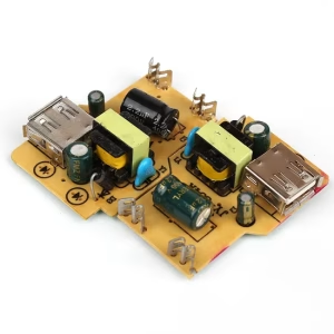
PCB Clone is an important reverse engineering technology in the electronics field. It refers to the process of fully copying an existing printed circuit board when the original design files are missing. The core goal of this technology is to achieve a 1:1 exact replica of the original board in form, function, and performance.
By nature, PCB cloning is not simple copying or imitation. It is a strict reverse engineering process. It starts with a physical circuit board and ends with a complete set of design files ready for production. These files include Gerber files, schematics, and Bill of Materials (BOM). Through PCB cloning, engineers can recover:
- Circuit net connections: Electrical connections between all components
- Component placement: Exact positions and orientation of each component on the board
- Board layer stack-up: Layer order, thickness, and materials for multi-layer boards
- Buried and blind vias: Complex via connections inside multi-layer boards
- Signal integrity features: Key signal trace lengths, impedance control, and other details
It is important to note that a responsible PCB cloning service always operates within legal boundaries. Professional service providers, such as ENA Electronics, ask customers to confirm before starting a project: whether the board to be cloned is obsolete or no longer supported by the original manufacturer, and whether the operation infringes on any valid patents or intellectual property rights. As FC PCBA states, PCB cloning is helping Chinese and global electronics companies improve their technical capabilities and break down technical barriers. However, it also calls for respect for intellectual property rights within the industry.
2 Advantages of PCB Cloning
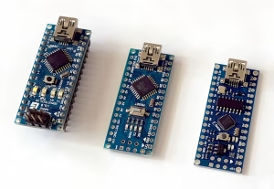
PCB cloning is widely used in industrial control, medical equipment, and aerospace because it offers clear benefits. These advantages help individual companies and also support the healthy growth of the electronics industry.
2.1 Shorten Time to Market
Time is very valuable in the fast-moving electronics market. Starting from zero with full R&D often takes too long. PCB cloning allows companies to complete product updates with the shortest time and lowest cost. Because the design is based on an existing mature product, quality is reliable. This helps companies seize market opportunities.
2.2 Improve Product Cost-Effectiveness
“High quality, low price” is the most notable feature of PCB cloning. With cloning technology, companies can produce fully functional boards at a lower cost. This makes the final product more acceptable to the mass market. It also brings more profit to companies and increases their competitiveness.
2.3 Support Secondary Development and Innovation
This is the key difference between PCB cloning and simple “copying.” The cloning process itself is a way to deeply understand the original design. After getting the full schematic and layout, engineers can perform secondary development:
- Remove functions– take out unneeded modules to lower cost
- Add functions– add new interfaces, higher processing power, or improved control systems
- Replace components– use modern parts that are easier to get, cheaper, or perform better
2.4 Solve Obsolete Component and Maintenance Problems
This is one of the most important real-world uses of PCB cloning. Many industrial machines, medical devices, and military systems depend on specific board designs. When the original maker stops production or a key chip becomes obsolete, the whole device may be thrown away. With PCB cloning, engineers can:
- Copy the whole boardfor use as a spare part
- Replace obsolete partswith current components to give old equipment new life
- Extract or rewrite firmware– for old ICs with missing code, observe input/output behavior or decode assembly code manually to rebuild the firmware
2.5 Speed Up Reverse Engineering and R&D Learning
When done legally, studying competitor or successful products is a shortcut to improving your own design skills. PCB cloning gives engineers a way to learn, analyze, and improve. By analyzing cloned schematics and layouts, companies can learn from others’ design work, avoid reinventing the wheel, and move faster in forward R&D.
| Dimension | Benefit | Typical Application |
| Time & Cost | Shorten launch time, lower R&D cost | Quickly follow market trends |
| Quality | Based on mature design, reliable | Make high-value consumer products |
| Maintenance | Solve obsolete part problems, extend life | Industrial, medical, military equipment |
| Innovation | Add or remove functions | Modernize old products |
| Learning | Legally analyze competitor designs | Technical research and training |
3 How to Copy a PCB?
Accurately cloning a PCB is a systematic project that requires careful work and patience. The whole process generally follows six core steps. Using ENA Electronics’ eight-step process as a reference, we can summarize it into six clearer stages.
3.1 Preparation and Documentation
- Target Board Assessment: First, check the PCB to be cloned for physical damage (such as burning or cracking). For a damaged board, a working board of the same model may be needed as a reference.
- Component List Documentation: Record the position, model, specification, and orientation of all components on the board in detail. For chips whose model cannot be read directly (such as ground-off or old ICs), record the pin count and package features.
- Equipment Preparation: Prepare high-resolution scanners (optical and X-ray), digital multimeter, capacitance meter, oscilloscope, soldering iron, desoldering wick, and professional CAD software (such as Altium Designer, Cadence Allegro).
3.2 PCB Scanning and Image Capture
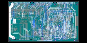
This is the key step to get digital information from the physical board.
- Surface Scanning: Use a high-resolution optical scanner to scan the Top Layer and Bottom Layer of the PCB to get clear images. Clean the board surface before scanning.
- Multi-Layer Scanning: For multi-layer boards (4 layers or more), X-ray scanning equipment is needed. X-rays can penetrate the outer copper and solder mask, clearly showing inner layer traces, power/ground plane splits, and connections of buried and blind vias. This step is critical for cloning high-density, high-complexity boards.
- Image Processing: Import the scanned images (usually BMP or PNG format) into PCB image processing software. Calibrate, align, reduce noise, and enhance contrast to prepare for trace extraction.
3.3 Schematic Recreation
This is the most technically demanding and time-consuming step in the whole cloning process. Engineers must act like “detectives,” tracing circuit connections based on the scanned images.
- Component Removal and Tracing: Remove all components one by one, then scan the “bare board” pad layers again. Compare the images with and without components to precisely identify which component and pin each pad belongs to.
- Net Tracking: In the CAD software, draw traces one by one based on the trace paths in the image. Start from a component pin, follow the copper trace until it connects to another component pin or via. This requires great patience and care.
- Hierarchical Restoration: First restore major functional blocks (such as power supply, microcontroller, interface drivers), then gradually refine the internal connections. Finally, form a complete netlist.
- Schematic Drawing: Based on the netlist and component information, draw the full electrical schematic in the schematic editor. For logic chips or programmable devices with unknown functions, it may be necessary to analyze their behavior through powered testing or a logic analyzer.
3.4 PCB Layout Design
With an accurate schematic, the next step is to restore the physical layout.
- Component Library Creation: Based on the actual size and package type of the removed components, create the corresponding component footprints in the CAD software. Ensure that pad positions and hole sizes exactly match the original PCB.
- Layout Restoration: Place the footprints at the correct coordinates. This step often uses the scanned image as a scale reference. Set the image as a semi-transparent background, then move the component footprints in the CAD software to align with it. Component position and rotation angle must be exactly the same as the original board.
- Trace Restoration: Route the traces in the CAD software’s routing layers according to the netlist from the schematic and the trace paths in the scanned image. For multi-layer boards, restore traces layer by layer and set vias correctly. Ensure inner layer trace directions and widths match the original.
- Design Rule Check: After completion, run DRC (Design Rule Check) to ensure there are no shorts, spacing violations, or other errors.
3.5 Prototype Manufacturing
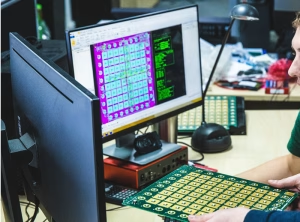
- Generate Production Files: Export the final PCB Layout design as Gerber files, drill files, BOM, and pick-and-place files.
- Board Fabrication and Component Sourcing: Send the Gerber files to a PCB manufacturer for prototyping. At the same time, purchase all components according to the BOM.
- Assembly: After receiving the bare PCB boards, solder all components according to the pick-and-place file and schematic. For small batches or prototypes, hand soldering may be used. For large batches, SMT placement machines are used.
3.6 Validation and Testing
This is the final checkpoint that determines the success of the cloning.
- Visual and Continuity Check: Check soldering quality. Use a multimeter to test for shorts on critical power rails.
- Functional Test: Install the cloned board into the original system and power it on. Compare its function with the original board. Test all interfaces, indicators, buttons, displays, etc., one by one.
- Performance Test: Use an oscilloscope, spectrum analyzer, or other equipment to test key signal parameters such as timing, voltage, frequency, and eye diagram. Compare them with the original board.
- Burn-in and Reliability Test: Run the cloned board under rated conditions for a long time to observe its stability.
The complete process is summarized in the table below:
| Step | Core Task | Key Tools/Skills | Deliverable |
| 1. Preparation | Assess board condition, document components | Visual inspection, multimeter | Component record sheet |
| 2. Scanning | Capture high-res images, multi-layer view | Optical/X-ray scanner, image software | Multi-layer bitmap files |
| 3. Schematic Recreation | Track nets, draw connections | CAD software (logic design), reverse thinking | Full schematic, Netlist |
| 4. PCB Layout | Restore footprints, re-route traces | CAD software (physical design), precise measurement | PCB design files, Gerber |
| 5. Manufacturing | Fabricate board, source parts, assemble | PCB factory, SMT or hand soldering | Cloned PCB prototype |
| 6. Test | Functional, performance, reliability validation | Oscilloscope, system-level test platform | Test report, qualified clone |
4 PCB Cloning Applications
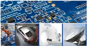
PCB cloning applications go far beyond simple “copying.” It has penetrated every corner of the modern electronics industry and has become an essential tool for solving real-world problems.
4.1 Industrial Control and Automation
Factory automation lines, CNC machines, PLC controllers, and other equipment have long life cycles. When their control boards stop being produced, the entire production line may face shutdown. PCB cloning provides the most economical and fastest spare part solution, ensuring production continuity.
4.2 Medical Equipment Maintenance
CT scanners, MRIs, ultrasound machines, patient monitors, and other medical devices are very expensive and require high reliability. When the original manufacturer no longer supplies a certain board or charges an extremely high price, hospitals or third-party maintenance companies can use cloning to get a functionally identical replacement board. This lowers maintenance costs and extends equipment life.
4.3 Communication and Network Equipment
Base station equipment, core routers, optical transmission equipment, and other communication devices also have long life cycles and hard-to-find spare parts. Cloning the specialized boards in these devices is an important way to keep communication networks running stably.
4.4 Military and Aerospace
Electronic systems in military equipment, satellites, and aircraft require long-term, reliable spare parts supply. Due to secrecy or discontinuation, many boards in older equipment cannot be obtained from the original source. PCB cloning (within legal and regulatory requirements) becomes a necessary means to ensure the readiness of defense equipment.
4.5 Consumer Electronics and Secondary Development
For learning and research, cloning classic game console motherboards or vintage computer boards helps enthusiasts understand classic designs and make improvements (such as adding HDMI output, USB ports, etc.). Some small and medium-sized companies also clone successful products on the market for rapid iteration and localized improvement, launching more competitive products.
4.6 Scientific Research and Education
In university labs or research institutions, researchers may need to conduct in-depth study based on an existing board that lacks design documents. Cloning technology turns the board into editable electronic files, making it convenient for simulation, modification, and teaching demonstrations.
5 Challenges in PCB Cloning Process
Although PCB cloning technology is mature, there are still multiple challenges in practice. Overcoming them requires professional knowledge, rich experience, and good equipment.
5.1 Legal and Intellectual Property Challenges
This is the primary challenge facing PCB cloning. Cloning a circuit board that is protected by patents or contains proprietary firmware without authorization is an infringement. Responsible cloning service providers ask customers for legal permission documentation, or only clone boards that are clearly obsolete, no longer supported by the original manufacturer, and do not infringe on others’ IP. “Legal use” is the foundation of the cloning service.
5.2 Technical Complexity Challenges
- High-density multi-layer boards: For 8-layer, 10-layer, or even more layers, the inner layer traces are very fine, and buried/blind vias are complex. Using X-ray to scan and accurately restore inner layer connections requires high equipment precision and engineer experience.
- Mixed-signal circuits: For boards containing both high-precision analog circuits (such as RF, small-signal amplifiers) and high-speed digital circuits, cloning must restore not only the connections but also the electromagnetic compatibility (EMC) design. This includes how analog and digital grounds are separated, component shielding, and trace impedance control. Otherwise, the clone may not work properly or may cause interference.
- Programmable devices and firmware: If the board has programmable devices such as microcontrollers, FPGAs, or CPLDs, the internal firmware is the “soul.” If it cannot be legally extracted from the original chip or its function reverse-analyzed, the cloned hardware is just an “empty shell.” While the firmware can be rewritten based on external behavior, the workload is huge and risky.
- Special process components: Some boards use custom thick-film circuits, hybrid ICs, or chips whose models have been ground off. Identifying the function and pinout of these components is a difficult reverse engineering task.
5.3 Quality Control and Reliability Challenges
- Component consistency issues: The original board may have used special batches, high-precision parts, or obsolete components. Finding replacements with exactly the same function, performance, and temperature characteristics is not easy. For example, if a replacement capacitor has a different ESR (Equivalent Series Resistance), the whole power supply filtering performance may degrade.
- Process consistency: The production process for the clone board (such as solder mask brand, copper thickness, surface finish) may be different from the original, potentially causing reliability differences in specific environments (high humidity, high temperature).
- Validation without design documents: Without original design specifications, the only way to verify that a clone board performs 100% like the original is to run both boards in the real system with extensive side-by-side testing. Any missed test scenario could hide problems.
6 FAQs
Q1: Is PCB cloning legal?
A: It depends on the purpose and the object. It is generally legal to: 1) Clone a board that you own and that has no IP disputes; 2) Clone a board that is obsolete, no longer supported by the original manufacturer, and does not infringe on any valid patent, for the purpose of maintaining your own equipment; 3) Use it for research and learning within legally allowed reverse engineering boundaries. It is illegal to clone boards protected by others’ patents or copyrights for commercial sale, or to copy boards containing proprietary encrypted firmware to break protection mechanisms. It is recommended to consult a legal professional before cloning.
Q2: How long does PCB cloning take?
A: The time varies greatly, mainly depending on board complexity:
- Simple boards(single/double-sided, <50 components, no ICs or simple ICs): About 1-3 working days
- Medium boards(2-4 layers, 100-200 components, including a microcontroller): About 1-2 weeks
- Complex boards(6+ layers, high density, BGA packages, containing programmable devices): May take 3-8 weeks or more, especially if firmware extraction or rewriting is required
Q3: How much does PCB cloning cost?
A: Cost is also related to complexity. It usually includes engineering fees (reverse analysis and design) and manufacturing fees. The following are approximate reference prices (RMB):
- Simple boards: Engineering fee about 800-3000 RMB
- Medium boards: Engineering fee about 3000-12000 RMB
- High-complexity boards(multi-layer, high density, firmware analysis needed): Engineering fee can be 15000-80000 RMB or higher
Per-unit manufacturing cost for batch production is separate. Most service providers give a fixed quote after evaluation.
Q4: Can I clone a PCB myself, or do I need professional service?
A: Hobbyists can certainly clone simple single/double-sided boards themselves. You need a scanner, a computer, free or low-cost PCB design software (like KiCad), and patience to manually trace and verify. However, for multi-layer boards, boards with BGA packages, high-speed signals, or that need firmware handling, it is strongly recommended to use a professional service. They have X-ray equipment, specialized copying software, signal integrity analysis experience, and firmware reverse engineering capabilities to ensure cloning success and long-term reliability.
Q5: How can I protect my own PCB product from being cloned?
A: You can use the following technical methods to increase the difficulty of cloning:
- Use security chips: Such as secure microcontrollers or cryptographic authentication chips (e.g., Maxim DS28E series), to implement dynamic password verification between the board and the main system
- Use trace obfuscation: Add non-functional “fake traces” on redundant layers, or use micro-blind vias to hide critical signals in inner layers
- Physical protection: Cover critical ICs with epoxy resin or special coatings to prevent probe access; use copper mesh to cover vias
- Chip marking removal: Grind off the model numbers on chip surfaces and replace them with non-standard markings
- Legal methods: File patents and trademarks, and sign strict Non-Disclosure Agreements (NDAs) with foundries and partners
Q6: If a cloned board does not work well, where could the problem be?
A: If a cloned board does not function correctly, common areas to check include:
- Schematic errors: A key node was missed or incorrectly connected during net tracking
- Component errors: The replacement component is not the correct type, especially for analog ICs, precision resistors, high-frequency capacitors, or crystals
- PCB layout differences: Component position or trace path differs too much from the original, causing timing, impedance mismatch, or crosstalk
- Missing/incorrect firmware: The main control chip is not programmed or the program is incomplete
- Soldering problems: Cold solder joints or bridges, especially under fine-pitch QFP or BGA devices
7 Summary
PCB cloning is a reverse engineering technology that has both practical value and technical depth. It is not simple “copying.” When done with respect for intellectual property rights, it is an effective tool for solving real-world problems such as equipment maintenance, obsolete spare parts supply, and old system upgrades. Through a strict six-step process (Preparation, Scanning, Schematic Recreation, Layout Restoration, Manufacturing, and Testing), professional engineers can create a 1:1 replica of the original board in form, fit, and function.
The value of PCB cloning is seen in many dimensions: it helps companies shorten time to market and reduce costs; it supports engineers in secondary development and innovation; it extends the life of expensive industrial and medical equipment. However, this field also faces challenges in legal ethics, technical complexity, and quality control. Choosing a legal, compliant, and technically capable professional service provider is the key to successful cloning. Understanding and properly using PCB cloning is an effective tool for solving complex hardware problems.
Related Posts
ORINEWPCB · PROJECT SUPPORT
Contact Us
Discuss your PCB assembly project with our team.
FREE QUOTE
Plan your turnkey PCBA build.
Share your quantity and requirements. Add Gerber files and a BOM when ready.
Files are optional for an initial discussion. Include any assembly, sourcing or testing requirements in your message.