
Mastering PCB Drilling: Your Guide to Precision Boards

Table of Content
- 1. The Foundation: What is PCB Drilling and Why It Matters?
- 2. Anatomy of PCB Holes: Types and Functions
- 3. PCB Drilling Methods: Mechanical vs. Laser
- 4. Essential Equipment for Precision Drilling
- 5. Key Considerations for Quality PCB Drilling
- 6. Common Drilling Challenges and Solutions
- 7. Best Practices for Optimal PCB Drilling
- 8. PCB Drilling FAQs
- 9. Summary
- Key Takeaways
In the intricate world of electronics manufacturing, the Printed Circuit Board(PCB) stands as the backbone of nearly every device we use. From smartphones to medical equipment, PCBs provide the structural and electrical foundation. A crucial, yet often underestimated, step in their fabrication is PCB drilling. Without precise holes, electronic components cannot be mounted, and electrical connections between layers remain impossible. For electrical engineers, hobbyists, and manufacturers alike, understanding the nuances of PCB drilling is paramount to creating high-quality, reliable circuit boards.
This comprehensive guide will demystify the PCB drilling process, covering everything from the fundamental importance of well-executed holes to advanced techniques like laser drilling for PCBs. We’ll explore the various types of holes, the machinery involved, common challenges, and best practices to ensure your PCBs meet the highest standards of precision and functionality. Whether you’re just starting with PCB projects or looking to refine your manufacturing game, mastering PCB drilling techniques is your key to elevating your electronic designs.
1. The Foundation: What is PCB Drilling and Why It Matters?
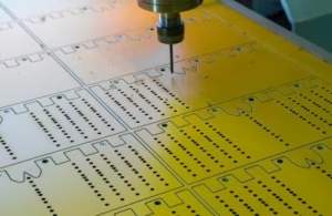
At its core, PCB drilling is the process of creating holes in a printed circuit board. These holes serve two primary functions:
- Component Mounting:They provide openings for through-hole electronic components(like resistors, capacitors, and integrated circuits) to be inserted and soldered, ensuring secure physical attachment and electrical connection.
- Electrical Connectivity:They form “vias”, which are crucial for establishing electrical connections between different copper layers within a multi-layer PCB, allowing complex circuits to be built in a compact space.
The importance of precise PCB drilling cannot be overstated. As electronic products become smaller, more complex, and demand higher performance, the accuracy and quality of these holes directly impact the board’s functionality and reliability. Poor drilling can lead to a host of problems, including misalignment of components, signal interference, shorts, opens, and even complete board failure. For electrical engineers, applying the right PCB drilling techniques is a critical differentiator between a functional prototype and a robust, mass-produced product. It’s a foundational step that sets the stage for the entire manufacturing process and the ultimate performance of the electronic device.
2. Anatomy of PCB Holes: Types and Functions
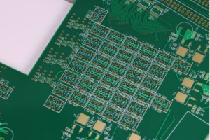
Not all holes in a PCB are created equal. Different types of holes serve distinct purposes, each critical to the board’s functionality. Understanding these types is fundamental to proper PCB design and manufacturing.
2.1 Plated Through Holes(PTHs)
Plated Through Holes(PTHs) are holes that are drilled through the entire PCB and subsequently plated with a conductive material(typically copper). This plating creates an electrical connection between all layers that the hole passes through. PTHs are commonly used for:
- Through-hole Component Leads:Providing a secure and conductive pathway for component leads to be soldered.
- Vias(Through-Vias):Creating electrical connections between any or all layers of a multi-layer board .
2.2 Non-Plated Through Holes(NPTHs)
Unlike PTHs, Non-Plated Through Holes(NPTHs) are drilled holes that do not receive a conductive plating. They are typically used for mechanical purposes, such as:
- Mounting Holes:Securing the PCB to an enclosure or chassis using screws.
- Tooling Holes:Used during manufacturing for alignment and indexing.
2.3 Vias: The Interconnect Highway
Vias are essentially plated holes that provide electrical connections between different layers of a PCB without necessarily being used for component mounting. They are crucial for creating compact, multi-layer designs.
- Through-Vias:These pass entirely through the PCB, connecting outer layers to inner layers and any intermediate layers. They are the most common type of via.
- Blind Vias:Drilled from an outer layer to an inner layer but do not pass through the entire board. They are “blind” from one side, saving space on the opposing outer layer.
- Buried Vias:Connect two or more inner layers of a PCB and are completely encapsulated within the board, invisible from the outer surfaces. These are essential for high-density interconnect(HDI) PCBs.
- Microvias:These are extremely small vias, typically less than 0.15mm(6 mils) in diameter, often created using laser drilling. They are crucial for HDI designs, allowing for very fine pitch components and increased routing density.
Here’s a comparison of common hole types:
| Hole Type | Description | Primary Function | Plating |
| Plated Through Hole(PTH) | Passes through all layers, inner wall plated. | Component mounting, electrical connection(through-via) | Yes |
| Non-Plated Through Hole(NPTH) | Passes through all layers, inner wall not plated. | Mechanical mounting, alignment | No |
| Blind Via | Connects an outer layer to one or more inner layers, not passing through completely. | Inter-layer electrical connection(space-saving) | Yes |
| Buried Via | Connects only inner layers, completely encapsulated within the PCB. | Inter-layer electrical connection(high-density) | Yes |
| Microvia | Very small diameter via, often laser drilled. | High-density inter-layer electrical connection(HDI) | Yes |
3. PCB Drilling Methods: Mechanical vs. Laser
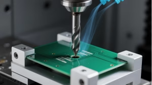
The choice of drilling method significantly impacts hole quality, precision, and cost. The two predominant methods are mechanical drilling and laser drilling, each with its own advantages and applications.
3.1 Mechanical Drilling(CNC Drilling)
Mechanical drilling, primarily performed using CNC drilling machines, is the most common and cost-effective method for creating standard PTH and NPTH holes. This process involves physically removing material using high-speed rotating drill bits made of tungsten carbide.
- Process:A multi-spindle CNC machine uses precise X-Y coordinates to position the PCB panel under the drill bits. The bits plunge through the board, creating holes. High spindle speeds(up to 2 00,000 RPM) and controlled feed rates are crucial to minimize burring and achieve clean holes.
- Advantages:Cost-effective for standard hole sizes, capable of drilling multiple layers simultaneously(stack drilling), mature technology.
- Limitations:Limited by drill bit diameter(cannot create extremely small microvias), wear and tear on bits(requiring frequent replacement), potential for mechanical stress, burring,or delamination, especially with small holes or exotic materials.
For hobbyists learning how to drill PCB at home, a simple drill press or even a handheld tool can be used, though precision will be significantly lower than industrial CNC machines.
3.2 Laser Drilling
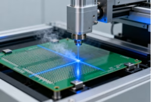
Laser drilling utilizes a high-energy laser beam to vaporize or melt material, creating holes without physical contact. This method is indispensable for HDI PCBs and applications requiring extremely small holes.
- Process:A focused laser beam ablates material layer by layer. Different laser types(CO2, UV, excimer) are used depending on the material and desired hole characteristics. CO2 lasers are often used for drilling dielectric materials, while UV lasers are preferred for metals and finer features due to their shorter wavelength and higher precision.
- Advantages:Capable of creating micro vias(as small as 20 microns), non-contact process(eliminates drill bit wear, mechanical stress, and burring), high precision and accuracy, ideal for blind and buried vias, suitable for various complex materials.
- Limitations:Higher initial equipment cost, generally slower for larger holes, heat-affected zone(HAZ) can sometimes be an issue for certain materials, not suitable for through-hole component mounting where larger diameters are needed.
3.3 Back Drilling
Back drilling is a specialized mechanical drilling technique used to remove the unused portion of a via stub. When a through-via connects only a few layers in a thick multi-layer board, the remaining “stub” acts as an antenna, causing signal integrity issues like reflections and impedance mismatches in high-speed applications. Back drilling removes this stub, improving signal performance.
4. Essential Equipment for Precision Drilling
Achieving high-quality PCB drilling requires specialized equipment, ranging from sophisticated industrial machines to more accessible tools for prototyping.
- CNC Drilling Machines:These are the workhorses of PCB fabrication. They feature multiple spindles, automatic tool changers, and high-precision motion control systems to drill thousands of holes accurately and repeatedly.
- Laser Drilling Systems:Employ various types of lasers(CO2, UV, excimer) to create microvias and complex hole geometries with extreme precision, particularly for HDI boards.
- Drill Bits:Typically made of tungsten carbide, these micro-tools are critical. Their quality, sharpness, and correct selection for material and hole size are paramount. They come in a vast range of diameters, often less than 1mm.
- Drill Press:For hobbyists and small-scale prototyping, a reliable drill press offers more stability and precision than a handheld drill, making it easier to achieve straight, clean holes.
- Micro-Drill Bits:Essential for hobbyists drilling PCB with a handheld tool for fine features.
5. Key Considerations for Quality PCB Drilling
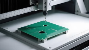
Several factors influence the quality and success of the PCB drilling process. Attention to these details is crucial for robust board performance.
- Aspect Ratio:Defined as the ratio of the hole depth to its diameter. High aspect ratios(e.g., 10: 1 or more) are challenging to plate reliably and can lead to plating voids or uneven copper thickness. PCB manufacturers often specify maximum aspect ratios for their capabilities.
- Drill Bit Selection and Maintenance:Choosing the correct drill bits size and type for the material(FR4, high-frequency laminates, etc.) is vital. Sharp, high-quality bits reduce burring and delamination. Regular inspection and replacement are critical.
- Speed and Feed Rates:The optimal balance between drill bit rotation speed(RPM) and downward feed rate determines drilling efficiency and hole quality. Incorrect settings can cause overheating, bit breakage, or poor hole wall quality.
- Drill Stack-up:In mechanical drilling, multiple PCB panels are often stacked together with entry and exit material(e.g., aluminum or phenolic resin) to protect the PCBs, ensure clean entry/exit holes, and extend drill bit life.
- Material Properties:Different PCB base materials(FR-4, high-frequency, flexible) have varying hardness, heat resistance, and abrasive properties, which dictate drilling parameters and tooling choices.
6. Common Drilling Challenges and Solutions
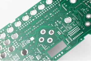
Even with advanced equipment, PCB drilling can encounter issues that compromise board quality.
1) Burring: Excess material around the hole edge.
- Solution:Optimize speed/feed rates, use sharper drill bits, ensure proper entry/exit materials, and implement deburring processes.
2) Delamination: Separation of layers within the PCB around the drilled hole.
- Solution:Control drill heat, use appropriate drill bits, and adjust feed rates.
3) Misalignment: Holes not accurately positioned according to the design.
- Solution:Regular calibration of CNC machines, precise panel registration, and robust jigging.
4) Hole Wall Roughness/Smear: Uneven or damaged inner surfaces of the hole, especially crucial before plating.
- Solution:Proper drill bit geometry, optimized drilling parameters, and effective desmear processes(chemical treatment to remove resin residue).
5) Broken Drill Bits: Leading to production halts and potential damage to the PCB.
- Solution:Correct speed/feed settings, proper drill bit quality and replacement schedule, and robust drilling equipment.
7. Best Practices for Optimal PCB Drilling
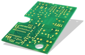
To ensure superior PCB drilling quality control, adhere to these best practices:
- Design for Manufacturability(DFM):Collaborate with your PCB manufacturer early on. Adhere to their specified minimum hole sizes, aspect ratios, and drill tolerances. Designing within capabilities prevents many drilling issues.
- Accurate Drill Files:Provide precise Gerber RS-274X format files, including drilling files(Excellon format is common), to the manufacturer. Any discrepancies can lead to critical errors.
- Tooling and Maintenance:Use high-quality, sharp PCB drilling tools and adhere to strict maintenance schedules for drilling machines. Regular calibration and inspection of drill bits are crucial.
- Environmental Control:Maintain a clean, temperature-controlled environment in the drilling area to minimize dust and ensure machine stability.
- Post-Drilling Inspection:Implement thorough inspection protocols, including visual inspection for burrs and delamination, and microscopic examination of hole walls to ensure cleanliness and readiness for plating.
- Process Optimization:Continuously monitor and optimize drilling parameters(speed, feed, peck depth) based on material types and drill bit characteristics.
8. PCB Drilling FAQs
Question 1: What is the difference between a PTH and an NPTH?
A PTH(Plated Through Hole) has its inner wall plated with conductive material to create electrical connections and allow component mounting. An NPTH(Non-Plated Through Hole) does not have plating and is used purely for mechanical purposes like mounting screws.
Question 2: Why is the aspect ratio important in PCB drilling?
The aspect ratio(hole depth to diameter) is critical because a higher ratio makes it more challenging to achieve uniform and reliable copper plating on the hole walls. Exceeding a manufacturer’s recommended aspect ratio can lead to plating defects and compromised electrical connections.
Question 3: When should laser drilling be used instead of mechanical drilling?
Laser drilling is preferred for creating very small holes(microvias), especially in high-density interconnect(HDI) PCBs, and for drilling blind or buried vias. It’s also chosen for delicate materials or when mechanical stress from drill bits needs to be avoided. Mechanical drilling is generally more cost-effective for larger, standard through-holes.
Question 4: What are vias used for?
Vias are used to create electrical connections between different copper layers of a multi-layer PCB. They allow complex routing and compact designs by providing vertical pathways for signals and power.
9. Summary
PCB drilling is far more than just punching holes in a board; it’s a precision art and science that underpins the reliability and functionality of nearly all modern electronics. From understanding the distinct roles of plated through holes(PTHs), non-plated through holes(NPTHs), and various vias, to choosing between the robust efficiency of mechanical drilling and the micro-precision of laser drilling, every step demands meticulous attention. Factors like aspect ratio, drill bit selection, and environmental controls are critical for preventing common issues such as burring, delamination, and misalignment. By embracing best practices, from DFM principles to rigorous post-drilling inspection, manufacturers and designers can ensure optimal quality control, leading to high-performance, durable printed circuit boards. Mastering PCB drilling techniques is not just about making holes; it’s about building a solid foundation for innovation in electronics.
As part of the same trusted team,we are excited to introduce our brand:OrinewPCB for faster,high-quality One-Stop PCB assembly services.
Key Takeaways
- Precision is Paramount:Accurate PCB drilling is fundamental for component mounting and creating reliable electrical connections, directly impacting board performance.
- Understand Hole Types:Differentiate between PTHs, NPTHs, and various vias(through, blind, buried, microvias) to specify the correct hole types for your design needs.
- Choose the Right Technique:Mechanical drilling is cost-effective for standard holes, while laser drilling is indispensable for microvias and HDI boards requiring extreme precision.
- Mind the Aspect Ratio:Be aware of the hole’s aspect ratio(depth to diameter), as high ratios can complicate plating and impact reliability.
- Implement Best Practices:Adhere to DFM guidelines, maintain drilling equipment, and conduct thorough inspections to mitigate common drilling problems and ensure high-quality output.








