
AI-Powered PCB Design: The Future of Electronics

Table of Content
- ۱. ظهور هوش مصنوعی در طراحی PCB
- نکات کلیدی
- ۲. چشمانداز در حال تکامل چالشهای طراحی PCB
- ۳. چگونه ابزارهای مبتنی بر هوش مصنوعی، طراحی PCB را متحول میکنند?
- ۴. مزایای کلیدی استفاده از هوش مصنوعی در طراحی PCB
- ۵. فناوریهای کلیدی هوش مصنوعی که نوآوری در PCB را هدایت میکنند
- 6ملاحظات اجرایی و چشمانداز آینده
- 7. طراحی برد مدار چاپی با هوش مصنوعی سوالات متداولs
- 8. خلاصه
1. The Dawn of AI in PCB Design
The intricate world of Printed Circuit Board(PCB) design has long been a domain of meticulous engineering, demanding precision, experience, and a deep understanding of complex electronic principles. As electronic devices become smaller, faster, and more powerful, the challenges associated with designing high-performance PCBs multiply exponentially. Miniaturization, higher operating frequencies, power integrity, signal integrity, and thermal management all contribute to a design process that is often time-consuming, error-prone, and resource-intensive. However, a transformative shift is underway with the advent of AI-powered optimization tools, fundamentally reshaping how PCBs are conceived, developed, and manufactured. These AI-driven PCB solutions promise to unlock unprecedented levels of efficiency, innovation, and reliability, pushing the boundaries of what’s possible in electronics.
Key Takeaways
- AI tools dramatically reduce PCB design cycle times and overall costs by automating complex optimization tasks.
- AI enhances critical design aspects like component placement, routing, signal integrity, power delivery, and thermal management.
- Integration of AI significantly improves Design for Manufacturability(DFM) and Testability(DFT), leading to higher first-pass yield and reduced rework in manufacturing.
- AI augments human designers, enabling them to focus on innovation while the AI handles computational complexities.
- The future of PCB design will see more sophisticated AI for multi-objective optimization and generative design, creating a more efficient and innovative development process.
2. The Evolving Landscape of PCB Design Challenges

Modern electronic products demand PCBs that are not just functional but also optimized across multiple dimensions. Designers grapple with a confluence of interconnected challenges:
- Increasing Complexity:Multi-layer boards, High Density Interconnect(HDI) designs, and embedded components make manual routing and verification incredibly difficult.
- Signal Integrity(SI) and Power Integrity(PI):High-speed signals are susceptible to crosstalk, reflections, and electromagnetic interference(EMI), requiring careful trace routing and impedance control. Ensuring stable power delivery across the board is equally critical.
- Thermal Management:Densely packed components generate heat, necessitating efficient thermal dissipation strategies to prevent performance degradation and component failure.
- Design for Manufacturability(DFM) and Testability(DFT):Designs must not only function but also be feasible to manufacture cost-effectively and easily testable, identifying potential issues early to avoid costly redesigns.
- Time-to-Market Pressures:The relentless pace of technological advancement demands shorter design cycles and rapid prototyping to remain competitive.
Traditional Electronic Design Automation(EDA) tools, while powerful, often rely on rule-based approaches or human intuition, which can fall short when faced with the combinatorial explosion of design possibilities. This is where AI-powered optimization tools step in, offering a paradigm shift.
3. How AI-Powered Tools Transform PCB Design?

AI’s strength lies in its ability to analyze vast datasets, identify complex patterns, and make intelligent decisions far beyond human cognitive capacity. In PCB design, this translates into powerful optimization capabilities across various stages:
1) Enhanced Efficiency and Speed
One of the most immediate impacts of AI is the drastic reduction in design cycle times. AI algorithms can rapidly explore millions of design permutations for component placement, trace routing, and layer stack-ups, identifying optimal solutions in minutes or hours rather than days or weeks. This acceleration is crucial for industries with tight deadlines and fast-evolving product roadmaps.
2) Optimizing Layout and Routing
At the heart of AI-driven PCB design is the intelligent optimization of PCB layout and routing. AI algorithms, particularly those leveraging machine learning and genetic algorithms, can:
- Automated Component Placement:Intelligently place components to minimize trace lengths, reduce noise, and improve thermal performance.
- Smart Routing:Generate optimal routing paths that adhere to design rules, minimize vias, avoid crosstalk, and maintain impedance control, even for high-density, multi-layer boards. This often outperforms human designers in complex scenarios.
- Layer Stack-up Optimization:Recommend the most efficient and cost-effective layer stack-up configurations for signal, power, and ground planes.
3) Ensuring Signal Integrity and Power Delivery
AI excels at predicting and mitigating SI and PI issues proactively. By analyzing design geometries, material properties, and operating frequencies, AI-powered PCB tools can:
- Identify potential impedance mismatches, reflections, and crosstalk early in the design phase.
- Optimize trace widths, spacings, and via structures to maintain signal quality.
- Design robust Power Delivery Networks(PDNs) that minimize voltage drop and ensure stable power to all components, crucial for high-performance processors and memory.
4) Thermal Management and Reliability
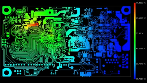
Heat is the enemy of electronics. AI can simulate complex thermal profiles and suggest optimal solutions to dissipate heat effectively:
- Component Placement for Heat Dissipation:AI can strategically place heat-generating components to leverage natural convection or integrate with cooling solutions.
- Via and Copper Weight Optimization:Recommend optimal via patterns and copper pour designs to enhance thermal conductivity.
- Predictive Failure Analysis:By analyzing design parameters and environmental conditions, AI can predict potential hot spots and areas of thermal stress, improving long-term reliability.
5) Design for Manufacturability(DFM) and Testability(DFT)
Bridging the gap between design and PCB manufacturing is critical. AI-powered tools can significantly improve DFM and DFT:
| Aspect | Traditional Approach | AI-Powered Approach |
| DFM Analysis | Rule-based checks, manual review, often late-stage feedback loops. Limited ability to identify subtle, complex issues. | Proactive, predictive analysis; real -time feedback during design. Identifies subtle manufacturing risks(e.g., acid traps, solder mask bridges) by learning from historical manufacturing data. |
| DFT Optimization | Post-design test point insertion, often adding cost and complexity. Limited fault coverage. | Optimal test point placement and design for in-circuit testing(ICT) or boundary scan. Maximizes fault coverage while minimizing test time and cost, reducing need for costly redesigns. |
| Yield Prediction | Based on historical data and expert judgment. | Predicts manufacturing yield based on design complexity, material choices, and known process variations, allowing for design adjustments before production. |
By integrating AI into these processes, designers can drastically reduce prototype iterations, decrease manufacturing costs, and accelerate the product’s journey from concept to market.
4. Key Benefits of Adopting AI in PCB Design
The strategic implementation of AI-powered optimization tools offers a multitude of advantages:
- Faster Time-to-Market:By automating repetitive tasks, accelerating optimization, and reducing design cycles, products can reach consumers significantly faster.
- Cost Reduction:Fewer design iterations, reduced prototyping, and higher first-pass yield in PCB manufacturing directly translate to lower development and production costs.
- Superior Performance and Reliability:AI’s ability to optimize for complex electrical, thermal, and mechanical parameters leads to PCBs with enhanced signal integrity, better thermal performance, and improved overall reliability.
- Democratizing Complex Design:AI can assist less experienced engineers in tackling complex design challenges, essentially embedding expert knowledge into the design tools.
- Innovation Catalyst:Freeing designers from tedious, repetitive tasks allows them to focus on innovation, exploring new architectures and technologies.
5. Key AI Technologies Driving PCB Innovation
The advancements in AI-powered optimization tools for PCB design are underpinned by several core technologies:
- Machine Learning(ML): Algorithms learn from vast historical design data to recognize patterns, predict optimal layouts, and identify potential issues.
- Deep Learning(DL): A subset of ML, deep learning, particularly with neural networks, excels at tasks like automated pattern recognition in complex layouts, making it ideal for component placement and routing.
- Generative Design: AI can explore millions of design permutations based on specified constraints and performance goals, generating novel and highly optimized solutions that human designers might not conceive.
- Reinforcement Learning:This allows AI systems to learn through trial and error, improving their optimization strategies over time by receiving feedback on the success or failure of their design choices.These technologies empower tools which natively integrate powerful AI capabilities to drive automation and refine layouts
6. Implementation Considerations and Future Outlook
While the benefits are clear , adopting AI-powered PCB design tools requires careful consideration. Data quality is paramount, as AI models learn from historical designs and manufacturing data. Integration with existing EDA ecosystems is crucial for a smooth workflow. Furthermore, designers will need to adapt their skills, shifting from manual rule-following to guiding and interpreting AI-generated optimizations. The future of PCB design is undeniably AI-driven. We can expect more sophisticated AI models capable of multi-objective optimization(e.g., simultaneously optimizing for cost, performance, and manufacturability), generative design where AI creates novel architectures, and greater synergy between AI and human designers, leading to an era of unprecedented innovation in electronics.
7. AI-Powered PCB Design FAQs
Question 1: What specific design aspects can AI-powered optimization tools improve?
AI tools can significantly improve component placement, trace routing, layer stack-up optimization, signal and power integrity, thermal management, and design for manufacturability and testability.
Question 2: How does AI reduce the time-to-market for PCBs?
AI reduces design cycle times by automating complex optimization tasks, rapidly exploring design alternatives, and reducing the need for multiple prototype iterations due to fewer design errors.
Question 3: Is AI replacing human designers in PCB design?
Not replacing, but augmenting. AI acts as a powerful co-pilot, handling repetitive and computationally intensive optimization tasks, allowing human designers to focus on creativity, architectural decisions, and critical problem-solving.
Question 4: What are the main challenges in implementing AI-driven PCB design?
Key challenges include ensuring high-quality and relevant training data, integrating AI tools seamlessly with existing EDA workflows, and the need for designers to develop new skills to effectively utilize and oversee AI-generated designs.
Question 5: Can AI optimize for both performance and cost simultaneously?
Yes, advanced AI algorithms are capable of multi-objective optimization, balancing conflicting parameters like performance, cost, manufacturability, and reliability to find the most balanced solutions.
Question 6: What skills do PCB designers need in the age of AI?
Designers will increasingly need to understand how to leverage AI tools effectively, interpret AI-generated suggestions, and validate their outputs. A strong foundation in design principles, critical thinking, and a willingness to adapt to new technologies will be crucial.
Question 7: How does AI improve signal integrity?
AI optimizes trace routing by considering factors like length matching, impedance control, crosstalk minimization, and proximity to sensitive components. It can automatically generate layouts that adhere to tight electrical constraints, significantly enhancing signal integrity.
8. Summary
The integration of AI-powered optimization tools is fundamentally transforming the landscape of PCB design. By leveraging advanced algorithms, these tools address the escalating complexities of modern electronics, offering unprecedented capabilities in speeding up design cycles, enhancing optimization of PCB layout and routing, ensuring robust signal and power integrity, and significantly improving thermal management. The benefits extend directly into PCB manufacturing, leading to higher DFM/DFT, reduced costs, and superior product reliability. As the industry moves towards increasingly sophisticated AI-powered PCB and AI-driven PCB solutions, the synergy between human expertise and artificial intelligence will continue to drive innovation, pushing the boundaries of what is achievable in electronics design.
OrinewPCB has focused as a one-stop PCB assembly manufacturer from PCB Manufacturing to Electronic Components Sourcing to PCB Assembly to Test to Program IC for more than 14 Years with reliable quality and fastest delivery for global clients.








