
A Complete Guide to Balancing Copper Weight and Trace Width in PCB Design

The use of copper in printed circuit board (PCB) design and production is a delicate fusion of exacting science and complex art. Finding the ideal balance between copper weight and trace width is crucial because it essentially dictates the circuit board’s ultimate performance, dependability, and cost. A skilled PCB design engineer must act like a master chef, precisely proportioning these two “ingredients” to “cook up” a stable and efficient circuit “feast.” This guide will systematically elaborate on the application and types of copper, trace design principles, and ultimately, how to achieve the best possible balance between them.
1. The Role of Copper in PCBs
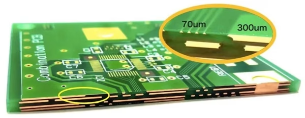
Copper serves as the “lifeblood” of a PCB, with its primary function being to carry and transmit electrical signals and power. Almost every electrical activity depends on the conductive pathways that copper creates.
- Signal Transmission:As signal traces, copper pathways are responsible for carrying high-frequency or low-frequency electrical signals between chips, connectors, and various components. Their quality, which includes things like crosstalk, signal attenuation, and impedance management, has a direct effect on signal integrity.
- Power Distribution:Acting as power and ground planes or wide traces, copper layers deliver stable, clean power to all active components on the board. Here, their current-carrying capacity is crucial.
- Thermal Management Path:Copper possesses excellent thermal conductivity. In power device design, copper foils are often used as thermal conduits, transferring heat generated by chips to larger copper areas or dissipating it through vias to other layers, thereby preventing localized overheating.
- Shielding and Reference Planes:Solid copper planes (e.g., power and ground planes) provide not only a stable voltage reference but also return paths for high-speed signals. Additionally, they act as electromagnetic shields, reducing Electromagnetic Interference (EMI).
It can be asserted that the essence of PCB design lies in the layout and configuration of copper foil, underscoring its immense importance.
2. Analysis of Copper Types and Their Processing
Copper foil used in PCB manufacturing is not monolithic; it is primarily categorized into two types based on deposition methods and processing techniques:
2.1 Rolled Annealed Copper
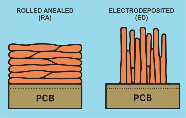
Characteristics: Produced by physically rolling high-purity copper cathodes into extremely thin foils. Its layered crystal structure gives it exceptional flexibility and ductility.
Applications: Primarily used in applications demanding high flexibility, such as Flexible Printed Circuits (FPCs) and rigid-flex boards. It also performs better when it comes to the skin effect in high-frequency circuits because of its smoother surface, which reduces signal loss.
Processing: In FPC manufacturing, RA copper undergoes specific chemical treatments and lamination processes to ensure strong adhesion to flexible substrates like polyimide.
2.2 Electrodeposited Copper
Characteristics: Formed through an electrochemical deposition process onto a rotating cathode drum.Compared to RA copper, it has a lower ductility but a higher hardness due to its columnar crystal structure. Because of the surface’s relative roughness, it adheres better to stiff substrates (like FR-4).
Applications: This is the most common and cost-effective type of copper foil used in rigid PCBs. It is extensively used in industrial controls, consumer electronics, and the majority of other general applications.
Processing: To improve adhesion to the substrate, one side of ED copper is typically treated to create a roughened profile (nodular structure). This roughness, however, can worsen signal loss in high-speed digital and high-frequency radio frequency designs. As a result, variations such as Very Low-Profile (VLP) and Low-Profile (LP) copper have been created, providing a better compromise between bond strength and surface roughness.
Copper Weight is typically measured in ounces per square foot (oz/ft²), referring to the weight of copper foil spread over a one-square-foot area. 0.5 oz, 1 oz, 2 oz, and 3 oz are common benchmarks. One ounce of copper has a thickness of about 35 μm (1.4 mil). The right copper weight must be chosen by designers in accordance with the requirements for thermal dissipation and current load.
3. Determinants of Trace Width Requirements
Another crucial factor in PCB design is trace width, which is determined by exacting engineering calculations and regulations rather than by chance.
- Current Carrying Capacity (Ampacity): This is the primary factor determining trace width.The current-carrying capability of a conductor is determined by the weight of the copper, the permitted temperature rise (such as 10°C or 20°C), and whether the trace is on an internal or exterior layer, as per the IPC-2152 standard, which amended the long-used IPC-2221. The minimal width for a given copper weight and temperature rise is usually found using standard charts or online calculators. For example, a width of roughly 60-80 mils (1.5-2.0 mm) may be needed for a 2A current with a 10°C temperature rise using 1 ounce copper.
- Impedance Control: In high-speed digital and RF circuits, the characteristic impedance of traces (e.g., 50Ω single-ended, 100Ω differential) must be precisely controlled. Trace width, copper thickness (also known as copper weight), dielectric material thickness, and its dielectric constant all affect impedance. To adhere to stringent impedance limits in this situation, trace width needs to be precisely determined using electromagnetic field solver software (such as Polar SI9000).
- Manufacturing Process Limits: PCB manufacturers have specific capabilities regarding minimum achievable trace width and spacing (trace/space).An excessively narrow trace design may result in a lower yield or possibly make the board unmanufacturable. To learn about the manufacturer’s process capabilities, it is imperative to speak with them in advance.
- Voltage Withstand (Creepage and Clearance): In high-voltage applications, sufficient distance must be maintained between conductors (creepage and clearance) to prevent arcing. Wide traces in crowded regions can jeopardize these necessary spacings, even though they are not directly related to width, therefore careful consideration is necessary.
4 Pros and Cons of Wide and Narrow Traces
4.1 Wide Trace: Pros and Cons
| Pros | Cons |
| High Current Capacity: Lower resistance allows for higher current carrying, preventing overheating. | Consumes Routing Real Estate: Quickly consumes valuable routing space and channels in high-density interconnect (HDI) designs. |
| Low IR Drop: Minimizes voltage drop over long-distance power distribution, ensuring adequate voltage at the end of the path. | Increased Difficulty in Impedance Control: Wider traces correspond to lower characteristic impedance, making it challenging to achieve target values in controlled impedance regions. |
| Superior Thermal Performance: Effectively draws heat away from dissipating components, especially when connected to large copper pours. | Potential for Increased Warpage: Uneven copper distribution across layers can contribute to PCB warpage during lamination or reflow soldering. |
| Enhanced Mechanical Strength: Less prone to breakage under mechanical stress. |
4.2 Narrow Trace: Pros and Cons
| Pros | Cons |
| Saves Routing Space: The most significant advantage, enabling more signal routes in a constrained area for high component density. | Limited Current Capacity: Higher resistance makes them prone to heating and unsuitable for power paths or high-current applications. |
| Facilitates Impedance Matching: More readily achieve standard impedance targets (e.g., 50Ω) for high-speed signals with specific dielectric thicknesses and copper weights. | Increased Signal Loss: Higher insertion loss at high frequencies due to the skin effect and reduced conductive cross-sectional area. |
| Essential for Fine-Pitch Components: Necessary to “escape” from the pin field of components like BGAs and QFNs with very small pin pitches. | Manufacturing Challenges and Cost: Places high demands on etching processes, potentially increasing scrap rates and manufacturing costs. |
| Mechanical Reliability Risk: More susceptible to damage during fabrication and assembly due to mechanical stress. |
5. Factors for Achieving the Optimal Balance
Finding the ideal ratio of trace width to copper weight is a multi-objective optimization procedure that necessitates careful evaluation and trade-offs between the following variables:
5.1 Prioritize Electrical Performance
Power Paths: First, determine the minimum width for power and ground traces based on the maximum continuous current and allowable temperature rise using the IPC-2152 standard. To save board space, increase the copper weight (for example, from 1 oz to 2 oz) for high currents instead of continuously enlarging the traces.
Signal Paths: For high-speed signals, start with impedance calculations to identify combinations of trace width, copper weight, and dielectric thickness that meet the target impedance. Here, copper weight and trace width are coupled as a “parameter set” serving the impedance goal.
5.2 PCB Layout Density
On boards with low component density, designers have greater freedom and can use wider traces and thicker copper for enhanced reliability.
In HDI designs, space is a premium resource. This often necessitates compromising on copper thickness (using standard 1 oz) and employing the minimum trace width within the manufacturer’s capabilities. In areas with dense power pins, techniques like using multiple power planes or embedded copper coins might be required to meet current demands.
5.3 Thermal Management Strategy
The overall thermal profile of the board must be assessed. For major heat sources, the underlying copper and connecting traces should be considered as heat sinks.One direct way to improve heat dissipation is to increase the weight of the copper and broaden the traces. In addition to guiding copper distribution and thickness selection, thermal simulation can assist in locating hot areas.
5.4 Manufacturing Cost and Process Capability
PCB manufacturing costs are increased with both finer trace widths/spacing (e.g., < 3/3 mil) and heavier copper foils (e.g., >3 ounce). The most popular, economical process combination that satisfies performance standards should be the design’s goal. It is essential to communicate with the manufacturer as soon as possible.
5.5 Reliability Requirements
Strict derating regulations are in place in industries with high reliability, such as aerospace and automotive. To endure harsh operating circumstances and guarantee long-term dependability, this frequently necessitates adding a 20%–50% margin to the determined minimum trace width and maybe employing thicker copper.
6. Q&A
Increasing the weight of copper is the main remedy. For instance, the current capacity almost doubles for the same trace width when going from 1 oz to 2 oz. Alternatively, to increase the overall cross-sectional area, think of routing the power trace on several layers and connecting them in parallel with several vias. Techniques such as embedding copper bars or inlays can be investigated for extreme situations.
Impedance calculations are based on ideal geometric models. Actual performance is also influenced by copper surface roughness, dielectric material consistency, the fiberglass weave effect, and proximity to other traces. Make sure you use the most recent field solver tools (like VLP) that take copper kind into consideration. Strict stack-up control and your manufacturer’s Design for Manufacturability (DFM) input are also very important.
Indeed, there is a notable distinction. IPC-2152 states that outer layer traces can carry greater current than inner layer traces for the same copper weight, trace width, and temperature rise. This is because interior layers are encased in dielectric material, which traps heat, whereas outside layers disperse heat more effectively (one side to air). Calculations must account for the layer location.
The following are the main scenarios: ① High-current applications, such as motor drivers and power modules (usually continuous currents exceeding 5A); ② Areas beneath components that dissipate power, where copper serves as a primary heat spreader; ③ Circumstances where mitigating voltage drop in power distribution networks requires lowering DC resistance; ④ Specific transmission lines and matching networks in high-power radio frequency circuits.
Generally, no. A solid, continuous ground plane inherently provides a very low-impedance return path. In the vast majority of applications, using the same copper weight for both signal layers and plane layers (e.g., all 1 oz) is standard practice. It would only make sense to think about thicker copper for planes in certain situations with very large return currents or when the ground plane acts as the main thermal channel.
7. Summary
In PCB design, balancing copper weight and trace width is not a straightforward binary decision; rather, it is a methodical engineering discipline that permeates every step of the design process. It requires that designers have a thorough understanding of how current, impedance, thermal management, and physical layout limitations interact.
A robust design workflow should be: Initiated by electrical requirements (current and impedance), constrained by physical space (layout density), used to determine a preliminary copper weight and trace width combination through calculation and simulation, subsequently refined considering thermal and reliability needs, and finally, validated and fine-tuned within the framework of Design for Manufacturability (DFM).
Gaining proficiency in this art of balance enables the designer to expertly negotiate the trade-offs between performance, cost, and reliability, identifying the ideal “sweet spot” to produce excellent PCB products that are stable, long-lasting, and functionally powerful.








