3D Solder Paste Inspection: What It Checks—and What to Specify
Short answer: 3D solder paste inspection (3D SPI) measures selected features of the paste deposit after printing and before component placement. Depending on the inspection system and program, those features can include deposit area, height, calculated volume, and position. SPI helps a team find print-process variation early; it does not prove that a finished solder joint is reliable or replace AOI, X-ray, or electrical testing.
Where 3D SPI fits in the SMT process
In a typical SMT line, solder paste is printed through a stencil onto PCB pads. SPI inspects the printed deposits before components are placed and before the board enters reflow. This timing matters: a print issue can be investigated while the relevant board, stencil, paste, and printer conditions are still identifiable. The exact line sequence and inspection coverage should be confirmed with the assembler for each build.
Three-dimensional inspection adds height information to image-based evaluation. An inspection program may evaluate pad-level or grouped deposits and compare measured features with programmed limits. “3D” does not mean every possible defect is automatically detected: board support, stencil and pad geometry, reflective surfaces, component/pad mapping, software settings, and the chosen acceptance criteria all affect what the report can establish.
What 3D SPI measures
At a practical level, SPI asks whether a printed deposit appears to match the programmed print target closely enough to continue under the agreed process rules. Inspection software commonly reports a combination of these feature types, subject to machine capability and program setup:
- Area or coverage: the measured footprint of the paste deposit relative to the programmed pad or aperture region.
- Height: the reconstructed height of the deposit at the measured location.
- Calculated volume: a system-derived value based on measured geometry; the calculation method and reporting units are system-specific.
- Position or offset: the location of the deposit compared with the programmed reference.
Typical print-related conditions to review include missing or insufficient deposits, excess paste, smear or bridging between neighboring deposits, and misregistration. A flagged measurement is an investigation cue, not automatically a confirmed defect. The program’s regions, reference data, thresholds, board support, and review rules determine what is flagged and how the line responds.
What SPI cannot verify
SPI inspects paste before components are placed. It therefore cannot directly confirm component presence or orientation, solder wetting, hidden-joint quality after reflow, electrical continuity, firmware behavior, or product-level function. A deposit that passes a programmed window is not proof that the completed assembly will meet every design or reliability requirement.
It also does not replace a process review. For example, a measurement can be misleading if the board is not supported consistently, the wrong variant or program is selected, the pad-to-aperture mapping is wrong, or the acceptance limits are not tied to the actual design and process. Treat SPI data as one checkpoint in a controlled build plan and agree how exceptions are reviewed.
SPI vs. 2D inspection, AOI, and X-ray
These methods answer different questions at different stages. The right inspection plan depends on package types, design risk, failure modes, customer acceptance requirements, and available access—not on selecting every method by default.
| Method | Typical timing | Main question | Important boundary | Useful RFQ detail |
|---|---|---|---|---|
| 2D paste inspection | After printing, before placement | Does the deposit image match programmed area/shape/position rules? | Does not provide the same height information as a 3D measurement system; capability varies by system. | Required pads/regions, image criteria, variants, and review response. |
| 3D SPI | After printing, before placement | Are selected deposit features such as area, height, calculated volume, or position within agreed limits? | Does not verify reflowed joints, component placement, electrical performance, or function. | Feature limits, coverage, false-call review, stop/reprint rules, and report evidence. |
| AOI | Commonly after placement or reflow, depending on line plan | Are visible component or solder-related features consistent with inspection criteria? | Optical line-of-sight and programmed coverage limit what can be observed; hidden joints need another method when warranted. | Inspection stage, visible feature coverage, package limitations, and defect disposition. |
| X-ray | After assembly, when package or risk warrants it | Can internal or obscured structures be evaluated for specified concerns? | Not a substitute for every electrical, functional, or reliability test; interpretation and acceptance basis matter. | Target packages, concern, sampling/coverage, acceptance reference, and image records. |
Use inspection methods as complementary evidence. For your board, ask the assembler to map each required failure mode to an inspection or test step, its coverage, and the disposition rule. OrinewPCB describes its PCB assembly factory and quality-control process; confirm the actual inspection sequence and scope for the specific project rather than assuming a webpage description defines a purchase-order acceptance plan.
How to turn an SPI result into action
- Confirm identity first. Match the board revision, panel/variant, stencil revision, paste, printer program, and inspection program to the released build package.
- Review the measurement context. Check board support, fiducials/reference alignment, pad/aperture mapping, inspected regions, units, and whether the result is per-pad or aggregated.
- Separate measurement from disposition. Define which results create a warning, trigger operator review, require cleaning or reprint, or stop the line. Do not assume a red/green screen is a complete acceptance specification.
- Look for patterns. A repeated shift across a panel, one component family, one stencil region, or one print interval can point to different process variables. Use production records and engineering review; do not change limits simply to make alarms disappear.
- Record the resolution. Capture the board/panel identity, program version, affected location, decision, rework or reprint action, and approval where required. Define whether representative images or a full data export are required.
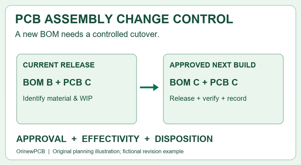
- Revalidate after changes. If the stencil, PCB, paste, variant mapping, or inspection program changes, agree which checks must be rerun before production continues.
These are planning prompts, not universal operating instructions. The assembler and customer should agree the actual limits and line response for the product, process, and risk.
What to specify in a PCBA RFQ
“Use 3D SPI” is not enough to define a measurable requirement. Include the intended evidence and how the team should act on an out-of-window result. If turnkey sourcing is in scope, align the SPI plan with the same released board revision, BOM/variant, and assembly package used for component procurement and production.
| RFQ item | Specify or provide | Why it matters |
|---|---|---|
| Build identity | PCB revision, panelization, assembly variants, quantity range, and applicable BOM release. | Prevents a correct inspection program from being applied to the wrong revision or variant. |
| Print definition | Stencil revision and available Gerber/ODB++ or other released fabrication data; identify known pad or aperture exceptions. | Pad-to-aperture relationships and design intent inform measurement regions. |
| Critical locations | List fine-pitch, small-aperture, thermal, bottom-terminated, or otherwise risk-relevant locations for engineering review. | Focuses coverage discussions; it does not prescribe one universal threshold for a package class. |
| Measured features | State whether the requirement concerns area, height, calculated volume, position, image review, or a documented combination. | “3D SPI” alone does not say which outputs are required or how they are calculated. |
| Limits and authority | Identify customer limits or the approval path for the assembler’s proposed limits; reference the applicable drawing/specification and revision. | Illustrations and generic limits should not silently replace product-specific written requirements. |
| Coverage and response | Define boards/panels and locations to inspect, sampling or full-coverage expectations, review/hold/reprint triggers, and deviation approval. | Measurement coverage and production disposition are separate decisions. |
| Evidence and retention | Specify required report fields, image/data format, traceability keys, record retention, and delivery timing. | Ensures the output can support the customer’s process review without implying that every raw sensor value is needed. |
A practical release check before the first build
- Are the PCB, stencil, BOM, variant, and inspection-program revisions aligned?
- Are critical locations and measured features agreed in writing?
- Are limits, warning/stop decisions, and exception approvals defined?
- Is the expected inspection evidence clear, including board/panel identifiers?
- Does the quote distinguish inspection coverage from AOI, X-ray, electrical, and functional-test requirements?
For a build that combines PCB fabrication, component sourcing, and assembly, send the released files and inspection expectations together. The turnkey PCB assembly service page explains the integrated scope; the project quote should still state its exact revision, quantities, inspection coverage, and acceptance evidence.
FAQs
What does 3D solder paste inspection check?
It evaluates programmed features of paste deposits after stencil printing and before placement. Depending on the system and program, outputs may include area, height, calculated volume, or position. Confirm the measured features, coverage, and limits with the assembler.
Can 3D SPI guarantee solder-joint quality?
No. SPI examines the printed paste before reflow; it does not directly verify the completed solder joint, electrical continuity, or product function. Use the inspection and test methods that address the product’s defined risks.
Is 3D SPI the same as AOI?
No. SPI focuses on printed solder-paste deposits before component placement. AOI inspects visible features at a later stage defined by the line plan. Their timing, targets, and limitations differ.
Does every PCBA project need X-ray if it uses SPI?
Not automatically. SPI does not inspect hidden joints after reflow. Whether X-ray is appropriate depends on packages, risks, customer requirements, and the agreed inspection plan. Define the target concern and acceptance basis in the RFQ.
Should an RFQ require 100% SPI?
Specify the required coverage explicitly, including whether it applies to every board/panel or selected locations and how exceptions are handled. The appropriate coverage is a project decision; do not infer it from the phrase “3D SPI.”
What files help an assembler plan SPI?
Provide the released PCB/panel data, stencil or paste-layer data when available, board and assembly revisions, BOM/variant mapping, critical-location notes, and written measurement/acceptance requirements. Ask the assembler to identify any data gaps before the build is released.
Related Posts
ORINEWPCB · PROJECT SUPPORT
Contact Us
Discuss your PCB assembly project with our team.
FREE QUOTE
Plan your turnkey PCBA build.
Share your quantity and requirements. Add Gerber files and a BOM when ready.
Files are optional for an initial discussion. Include any assembly, sourcing or testing requirements in your message.