
AI PCB Design Considerations and Requirements Management

As we move through 2025–2026, the PCB industry is undergoing a structural transformation. The primary driver has shifted from traditional consumer electronics cycles to the long-term demand generated by AI computing infrastructure.
AI servers, GPU clusters, data center switches, and high-bandwidth memory systems are pushing PCB technology to unprecedented limits:Signal frequencies moving from 10Gbps to 112Gbps;Power consumption jumping from tens of watts to kilowatts;PCB layer counts rising from 8 to over 40;Base materials upgrading from standard FR-4 to low-loss, high-speed CCL systems.At the same time, the upstream supply chain—CCL, copper foil, and glass fabric—is being rapidly absorbed by AI demand, creating a clear structural shortage.
Therefore, an AI PCB is no longer just a design problem. It is a three-in-one systems engineering challenge combining design capability, material systems, and supply chain management.
1 Defining the AI PCB: From “Electronic Board” to “Computing Carrier”

An AI PCB (Artificial Intelligence Printed Circuit Board) refers to a high-performance printed circuit board used in AI computing systems. Core applications include:AI training servers (GPU/TPU clusters);High-speed interconnect switches (800G/1.6T networks);PCIe Gen5 / Gen6 accelerator cards;HBM high-bandwidth memory systems;Edge AI inference devices
1.1 A Fundamental Shift in Purpose
The goal of a traditional PCB is straightforward: “Transmit electronic signals reliably.”The goal of an AI PCB has evolved into: “Maintain system-level stability under extreme power consumption and ultra-high-speed conditions.”
This means the PCB has changed from a passive carrier into an active bottleneck controller for system performance.
1.2 Three Structural Changes
- Signal Frequencies Enter the Millimeter-Wave Realm
Speeds have moved from PCIe 4.0’s 16GT/s to PCIe 5.0’s 32GT/s, PCIe 6.0’s 64GT/s, and Ethernet links using 112G PAM4. At these frequencies, transmission line losses spike. Reflection problems cause inter-symbol interference over very short distances. The dielectric properties of the material become the primary limiting factor for signal integrity.
- Power Density Grows Exponentially
A single AI GPU now consumes between 400W and 1200W. A fully loaded AI server rack can draw 10kW to 100kW. This presents two major headaches for PCB design: extremely high current density and severe localized hot spots directly under the chips.
- A Generational Shift in Material Systems
The material set for AI PCBs is migrating away from FR-4 toward: Low-loss CCL, resin systems with high Tg (over 180°C), T-glass fabrics for better mechanical stability, and high-thermal-conductivity composites.
2 AI PCB vs. Traditional PCB: An Engineering-Level Comparison
| Dimension | Traditional PCB | AI PCB |
| Application | Consumer electronics | AI/HPC/Data Center |
| Layer Count | 2–8 layers | 12–40+ layers |
| Signal Speed | <5Gbps | 56–112Gbps |
| Impedance Control | ±10% | ±5% or tighter |
| Base Material | FR-4 | Low-loss CCL |
| Thermal Design | Passive cooling | Active thermal management |
| Manufacturing Difficulty | Moderate | Extremely high |
- The Core Essence
The difficulty with an AI PCB isn’t just that it’s “more complex.” The real challenge is managing a multi-physics coupled constraint system where Signal Integrity (SI), Power Integrity (PI), and Thermal Management clash and interact, all governed by the chosen materials.
3 AI PCB Design Considerations

3.1 High-Speed Signal Integrity (SI) Design
Loss control is the central problem for high-speed signals.
(1) Sources of Signal Loss
Total insertion loss comes from four main sources:
- Dielectric Loss:The dominant loss at high frequencies, proportional to the material’s dissipation factor (Df).
- Conductor Loss:Caused by the skin effect and copper surface roughness. Rougher copper creates a longer effective path and more loss. HVLP (Hyper Very Low Profile) copper is essential.
- Reflection Loss:Caused by impedance discontinuities at vias, connectors, or line width changes.
- Via Structure Loss:The unused portion of a through-hole via barrel (the stub) causes resonant effects at high frequencies.
(2)Impedance Control
Differential pairs typically require strict control to 85Ω or 100Ω, with an error margin held within ±5%. This tight tolerance is critical for a low Bit Error Rate (BER).
(3)Key Design Techniques
- Backdrilling:This process removes the conductive via stub that causes destructive resonances. It is a must-have technique for reliable 112Gbps signal transmission. The design must allow physical space for the backdrill and define precise depth tolerances.
- Differential Pair Routing:Pairs must be routed with tight physical and electrical length matching. The timing mismatch (skew) must be kept very small, typically under 5ps. When changing layers, symmetric return-path vias must be placed next to the signal vias.
- Return Path Continuity:High-speed return current always follows the path of least inductance—the reference plane right next to the signal trace. Never route a critical high-speed signal across a split in its reference plane. This is a basic but critical rule that prevents major EMI and signal integrity failures.
3.2 Power Integrity (PI) Design
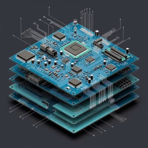
The high power draw of AI chips makes power delivery network (PDN) design a core stability issue.
(1)PDN Design Challenges
Today’s AI chips operate at core voltages below 0.8V while demanding hundreds of amps. This creates two big problems: massive IR drop from tiny resistances, and the need for an ultra-fast transient response that can handle huge current steps within nanoseconds.
(2) Voltage Drop and Target Impedance
The voltage drop follows a simple physical model: Vdrop=I×RVdrop=I×R. The core job of PDN design is to lower this “R” by creating a low-impedance path from the voltage regulator module (VRM) to the chip pads. Key tactics include using 2oz or thicker copper planes, using multiple parallel power vias to reduce connection inductance, and using tightly coupled power-ground plane pairs (thin dielectric) to create planar capacitance, which helps suppress high-frequency noise.
(3)Decoupling Strategy
A robust decoupling strategy uses a multi-tier capacitor network:
- Chip/Package-level capacitancehandles GHz-range transients.
- High-frequency decoupling:Small (0201/01005) 0.01–0.1µF MLCCs placed directly under the BGA.
- Mid-frequency decoupling:1–10µF MLCCs to suppress PDN resonance peaks.
- Bulk decoupling:Larger 100µF+ capacitors spread across the board to supply the main charge during current steps. This forms a wideband filtering network that covers from KHz up to hundreds of MHz.
3.3 Thermal Management
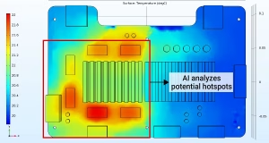
Thermal issues have become one of the top causes of AI PCB design failures.
(1)Heat Density Problem
The local heat flux under a GPU or CPU die can exceed 100W/cm², with hot spot temperatures hitting 90°C–120°C. This hurts chip performance and lifespan. It also causes problems with CTE (Coefficient of Thermal Expansion) mismatches, which can lead to solder joint fatigue and board delamination.
(2)Thermal Path Design
The goal is to build the lowest possible thermal resistance path from the chip junction to the ambient environment. The physical basis is simple: Rth=ΔT/PRth
- Vertical Paths:Place a dense array of thermal vias filled with a conductive material directly under the hot component to pull heat down into inner copper layers or the backside of the board.
- In-Plane Spreading:Use embedded copper coins (T-Coins or C-Coins) that are pressed into the PCB and make direct contact with the component, spreading heat efficiently across the plane.
- Copper Weight:Move to 3oz or even 6oz copper on power and ground planes to improve lateral heat spreading.
- System-Level Alignment:The PCB thermal design must align with the system-level cooling solution, whether it’s forced-air heatsinks, cold-plate liquid cooling, or immersion cooling.
3.4 Material Selection: The Most Critical Strategic Risk
Heading into 2026, the biggest bottleneck for an AI PCB project often isn’t the design file; it’s the materials buyer.
(1)Current Supply Chain State
Lead times for high-end, low-loss CCL (like Panasonic M6/M7 grades) have stretched to 4–6 months. This is because material suppliers allocate their limited production capacity to major AI clients first. The glass fabric used inside these laminates is also in short supply. PCB materials have entered a “strategic resource” phase.
(2)Material Selection and Performance Needs
- CCL:For 112Gbps signals, you need an ultra-low-loss CCL with a Df of less than 0.003 at 10GHz. For 56Gbps, a very-low-loss material with a Df between 0.004 and 0.006 might work. The glass transition temperature (Tg) of the material must be above 180°C to survive lead-free assembly processes.
- Copper Foil:Must be HVLP or smoother to minimize conductor loss. Outer layer thicknesses may need to be 2-3oz, and inner layers 1-2oz, depending on current-carrying requirements.
- Glass Fabric:To avoid the “fiber-weave effect” that causes impedance variations and skew, the fabric must be very uniform. This means using spread glass or flat glass cloth.
3.5 DFM and Manufacturing Feasibility
A complex AI PCB design cannot be created in a vacuum. A deep, front-loaded Design for Manufacturing (DFM) review with the fabricator is essential. Key areas to negotiate and assess include: the reliability of high-aspect-ratio laser-drilled microvias; warpage control during the lamination of 40+ layers; the fabricator’s ability to hold impedance tolerances given the statistical variation of line widths and dielectric thickness in mass production; and the use of process coupons and step-lamination strategies needed to yield such a complex board.
4 Supply Chain Reality: AI-Driven Structural Changes
AI is reshaping supply and demand at a fundamental level.
- AI Demand Squeezing Global Capacity:PCB fabricators prioritize capacity in this order: AI-GPU server boards first, high-speed network switch boards next, and then everything else. Capacity for other long-running programs in the industrial and automotive sectors is being squeezed out.
- Material Costs on an Upward Path:The price of CCL has risen 20-40% year-over-year. Copper prices are volatile, and specialized foils are even tighter. A structural shortage of electronic-grade glass fabric runs through the whole chain.
- Geopolitical Factors:The supply of some key chemical resins is unstable due to trade policies and geopolitical conflicts. Rising global energy costs increase the cost of everything from copper smelting to final lamination.
- Industry Logic Has Shifted:The PCB industry is moving from a volume-driven, cost-optimization model, to an “AI computing-driven” model, where technical capability in materials and simulation is the true barrier to entry.
5 OEM / EMS Strategies: Management & Procurement
System builders must shift from tactical buying to building resilient supply chains.
- Material Locking Strategy:Lock in capacity and pricing with a long-term agreement for the core, high-end CCL 6–12 months in advance. Develop a qualified multi-vendor system and hold 45–90 days of safety stock for key materials.
- Design and Supply Chain Collaboration:Engineering must drive procurement decisions with an “early collaborative material selection” process. Teams should design in qualified alternative materials from the start, performing a real BOM risk analysis for single-source components and qualifying a backup laminate as a risk buffer.
- Digital Supply Chain Management:Use predictive tools to model internal demand and monitor supplier lead time trends in real time. A multi-site production strategy can shift builds to different regions if a local supply shock occurs.
- Shift from Cost to Assurance:The primary goal for the next 2-3 years must move from cost optimization to supply assurance. Paying a premium for a strategically secured allocation is a small price to pay to protect a product’s launch window and market share.
6 FAQs
Q1: Why are AI PCBs so difficult to make?
Because it’s not a single problem. It’s the tightly coupled, interactive challenge of high-speed signal integrity, high-current power delivery, extreme thermal management, and the selection and procurement of strategic, scarce materials.
Q2: What is the biggest bottleneck for AI PCBs right now?
It’s not pure circuit design. It’s the availability and predictability of the supply of high-end, low-loss materials. The ability to secure a stable, high-quality material supply is itself the highest competitive barrier.
Q3: How long will this material shortage last?
This is a structural bottleneck. New capacity for chemical synthesis, glass yarn spinning, and copper foil production takes years to bring online. The industry expects this high-pressure supply situation to persist for at least 2–3 more years.
Q4: Can a typical PCB shop enter the AI market?
The barriers are very high. Beyond the capital equipment investment, a shop must build proficiency in high-speed simulation, advanced backdrilling and high-aspect-ratio manufacturing, cleaner cleanroom environments, and must acquire a team with deep knowledge of high-speed material science.
Q5: Are AI PCBs more profitable?
The gross margin looks better on a calculator, but the risks are also much higher. High R&D and NRE costs, the depreciation of high-end equipment, high scrap costs if yields are missed, and the carrying cost of strategic inventory make actual free cash flow heavily dependent on perfect execution.
Q6: What’s the future trend for the PCB industry?
A very clear trend toward high-end consolidation. The few fabricators who can serve AI and HPC customers reliably will capture the bulk of the industry’s profit, creating a positive feedback loop. Mid- and low-end shops will face increasingly fierce, commodity-based competition.
7 Summary
AI PCBs are reshaping the entire PCB industry chain. The core changes are:
- Technological Upgrade:High speed (112Gbps+), high power (kW-level), and high density are the new standard. Design is a multi-physics art.
- Materials Become the Core Bottleneck:CCL and glass fabric have become strategic resources. Locking down materials means locking in your future.
- Supply Chain Restructuring:AI computing demand is now the force that determines PCB capacity allocation globally.
An AI PCB isn’t just a technology upgrade; it represents a structural turning point as the PCB industry enters the “Age of Computing Infrastructure.” In this shift, only companies that can deeply integrate advanced engineering design, strategic material management, and a resilient supply chain can master this complexity and become the new leaders of the industry.
OrinewPCB has focused as a one-stop PCB assembly manufacturer from PCB Manufacturing to Electronic Components Sourcing to PCB Assembly to Test to Program IC for more than 14 Years with reliable quality and fastest delivery for global clients.








