
PCB Impedance Control: To Ensuring Signal Integrity

Table of Content
In the landscape of modern electronics, the demand for faster data rates and higher frequencies is relentless. We have moved far beyond the era where a Printed Circuit Board (PCB) was merely a green fiberglass plate used to mechanically support components. Today, as signal frequencies frequently cross the 100 MHz, 1 GHz, and even 10 GHz thresholds, the copper traces on a board cease to behave like simple wires. Instead, they act as transmission lines.
At these speeds, the electrical properties of the board itself—specifically its impedance—become the deciding factor between a high-performance product and a prototype that fails intermittently or fails EMI/EMC testing entirely. This guide provides an exhaustive look into PCB Impedance Control, exploring why it matters, how it is calculated, and how you can ensure your manufacturer delivers exactly what your high-speed design requires.
1. What is Impedance?
To understand impedance control, we must first distinguish between Resistance and Impedance.
(1)Resistance (R) is a concept tied to Direct Current (DC). It is the opposition to current flow based purely on the material’s properties (like copper resistivity) and its cross-sectional area. In a DC circuit, resistance is constant regardless of time or frequency.
(2)Impedance (Z), however, is a “complex” quantity used in Alternating Current (AC) circuits. It is the total opposition a circuit offers to the flow of energy at a specific frequency. It is mathematically represented as a combination of:
- Resistance (R):The real part of impedance.
- Reactance (X):The imaginary part, which consists of Inductive Reactance (XL) and Capacitive Reactance (XC).

On a PCB, every trace has a parasitic inductance (due to its length and the magnetic fields it creates) and a parasitic capacitance (due to its proximity to other copper layers and the dielectric material between them). When a high-speed signal travels down a trace, it “sees” this combination of R, L, and C. If these values are consistent along the entire length of the trace, the signal flows smoothly. If they change, the signal encounters an “impedance discontinuity,” leading to energy reflections.
2. How is Impedance Determined?
Determining the characteristic impedance of a PCB trace is a balancing act of several physical variables. It is not just about the trace itself, but the entire environment surrounding the copper.
2.1Trace Width (W)
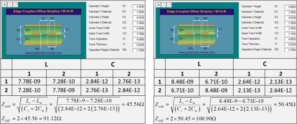
The width of the copper trace is the most common variable designers adjust. There is an inverse relationship: as trace width increases, impedance decreases. This is because a wider trace has higher capacitance to the reference plane.
2.2 Copper Thickness (T)
Measured in ounces (oz) or microns (μm), the thickness of the trace also affects impedance. Thicker copper leads to lower impedance, though its impact is usually less dramatic than changes in width.
2.3 Dielectric Thickness (H)
This is the distance between the signal trace and the nearest reference (ground or power) plane. As the distance between the trace and the plane increases, the impedance increases. This is a critical factor in “stackup design.”
2.4 Dielectric Constant (ϵr or Dk)
The Dk of the PCB material (like FR-4, Rogers, or Megtron) measures how much electrical energy the material can store. A higher Dk increases capacitance and thus lowers the impedance. Standard FR-4 has a Dk around 4.2 to 4.5, while high-frequency materials may have a Dk as low as 3.0.
2.5 Trace Geometry (Microstrip vs. Stripline)
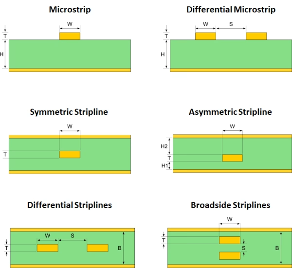
- Microstrip:A trace on the outer layer with one reference plane below it.
- Stripline:A trace embedded in an internal layer, sandwiched between two reference planes. Striplines generally require narrower traces to achieve the same impedance as microstrips because they have double the capacitive coupling.
3. What is Impedance Control and Signal Matching?
Impedance Control is the practice of deliberately designing a PCB so that the characteristic impedance of specific traces stays within a tight tolerance (usually ±10% or ±5%).
Signal Matching (or Impedance Matching) is the process of ensuring that the impedance of the source (the chip driving the signal), the transmission line (the PCB trace), and the load (the receiving chip) are all equal.
The “Maximum Power Transfer” Principle
In physics, maximum power is transferred from a source to a load when their impedances are matched. In digital electronics, if a driver has an output impedance of 50 Ω, and it sends a signal into a 75 Ω trace, the signal will not be fully absorbed by the trace. A portion of the voltage wave will “bounce” back toward the source. This is known as a reflection.
If the signal matches the trace impedance, the energy flows through like a wave in a perfectly straight, smooth pipe. If there is a mismatch, it’s like a wave hitting a wall—the resulting interference can destroy the logic levels of your data.
4. Why Control Impedance on PCBs?
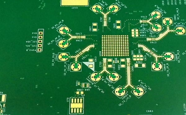
In low-speed designs (e.g., a simple Arduino project running at 16 MHz), the “electrical length” of the trace is much shorter than the wavelength of the signal. In these cases, impedance doesn’t matter much. However, in high-speed designs (DDR RAM, PCIe, USB 3.0, HDMI), impedance control is mandatory for the following reasons:
l Eliminating Signal Reflections
Reflections cause “ringing”—oscillations at the edges of digital pulses. If the ringing is severe enough, the voltage might cross the threshold between a logic ‘0’ and a logic ‘1’ multiple times during a single clock cycle, causing double-triggering or data corruption.
l Minimizing Electromagnetic Interference (EMI)
When impedance is not controlled, the energy that isn’t transmitted correctly often radiates outward as electromagnetic noise. This can cause your device to fail FCC or CE certification, and it can also interfere with other sensitive components on your board.
l Maintaining Signal Timing
High-speed data protocols rely on precise timing. Impedance affects the propagation delay (the speed at which the signal moves). If two traces in a differential pair have different impedances, the signals will arrive at different times (skew), leading to a failure in data recovery.
l Avoiding “Mystery” Failures
Uncontrolled impedance issues often manifest as intermittent bugs. A device might work at room temperature but fail when it gets warm (because Dk changes with temperature), or one batch of boards might work while another doesn’t. Controlling impedance ensures consistency across thousands of manufactured units.
5. How to Calculate PCB Trace Impedance?
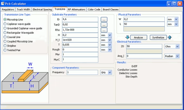
Manual calculation of impedance is notoriously complex because it involves solving field equations for specific geometries. Most designers rely on the following methods:
- Advanced CAD Tools:Professional software like Altium Designer includes integrated field solvers that calculate impedance automatically based on your stackup.
- Manufacturer Calculators:Since every fabricator has unique material stocks and tolerances, using a manufacturer’s tool—such as the JLCPCB Impedance Calculator
- Key Inputs for Calculation:
Trace Type: Microstrip, stripline, or differential pairs26.
Dimensions: Trace width, thickness, and spacing
Material Specs: Dielectric constant and dielectric height
6. Advanced Methods to Achieve Impedance Matching
Achieving a target impedance in a CAD tool is only the first step. In the real world, routing high-density boards requires sophisticated strategies to maintain that impedance from the driver pin to the receiver pad.
6.1 Advanced Termination Strategies
When the native output impedance of an IC does not match the PCB trace, termination is required:
- Series Termination:A resistor is placed as close to the source as possible. This is the most common method for CMOS logic and DDR clocks because it consumes very little power.
- Parallel Termination:A resistor is placed at the end of the line, tied to GND or a termination voltage. While it effectively swallows reflections, it results in constant DC power consumption.
- Thevenin Termination:Using a resistor divider at the load to provide both impedance matching and a specific DC bias level for the signal.
6.2 Differential Pair Precision
High-speed protocols like PCIe, SATA, and HDMI rely on differential pairs.
- Intra-pairSkew: The two traces in a pair must be length-matched to within a few mils. Any mismatch converts the differential signal into a common-mode signal, causing EMI.
- Tight vs. Loose Coupling:Tight coupling (small spacing between traces) makes the pair more immune to external noise but makes the impedance more sensitive to manufacturing tolerances in trace width.
6.3 Solving the “Return Path” Problem
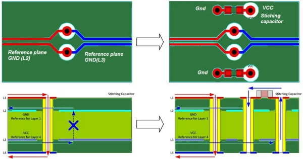
Every signal is a loop. The current flows out the trace and must return via the ground plane.
- Split Planes:If a high-speed trace crosses a gap in the ground plane, the return current must take a long detour. This increases loop inductance, causing a massive impedance spike and turning the board into a radio antenna.
- Stitching Capacitors:If you must switch reference planes (e.g., from a GND plane to a VCC plane), you must place a decoupling capacitor nearby to provide a high-frequency bridge for the return current.
6.4 Skin Effect and Surface Finishes
At multi-gigahertz frequencies, electrons only travel on the very outer “skin” of the copper.
- Copper Roughness:Standard copper foil has a “tooth” to help it stick to the fiberglass. This roughness increases the path length for electrons, effectively increasing resistance and changing impedance.
- ENIG vs. Immersion Silver:Electroless Nickel Immersion Gold (ENIG) includes a layer of nickel, which is magnetic and high-loss at high frequencies. For signals above 5GHz, Immersion Silver or OSP is preferred to maintain impedance stability.
7. Impedance Control Verification: Closing the Loop
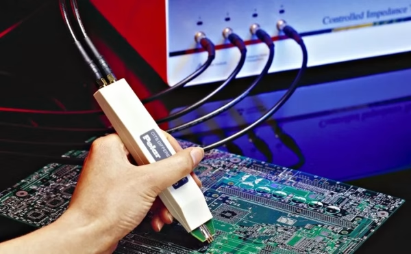
Designers must verify that the “as-built” board matches the “as-designed” file.
7.1 Pre-Production Engineering (EQ)
Before a single board is etched, the manufacturer performs a “Front-End Engineering” review. They will compare your requested stackup with their available material stocks. If you requested a 4.0 mil trace for 50 Ω but their material has a slightly different Dk, they will adjust your trace width (usually by ±0.5 mil) and ask for your approval.
7.2 The Test Coupon
Since you cannot easily probe the internal layers of a finished PCB without destroying it, manufacturers add a Test Coupon to the edge of the panel. This coupon is a 10cm-long strip that replicates the exact stackup, trace width, and spacing used in your design.
7.3 Time Domain Reflectometry (TDR) Testing
The “Gold Standard” for verification is the TDR.
- How it works:A TDR sends a fast-rise-time step pulse down the test coupon. Any change in impedance causes a reflection.
- The Output:The machine generates a graph showing impedance vs. distance. If the graph stays within your specified ±10% window, the batch is passed. If there is a “dip” or “spike,” the manufacturer knows exactly where the etching or pressing process went wrong.
8. Specifying Impedance Requirements for Manufacturers
Poor documentation is the cause of impedance failure. To ensure success, follow these documentation standards:
8.1 The Detailed Stackup Drawing
Provide a diagram that specifies:
The exact layer order.
- Material types (e.g., FR-4 High-Tg, Rogers 4350B).
- Required thickness for each Core and Prepreg layer.
- Finished copper weights (e.g., 1oz outer, 0.5oz inner).
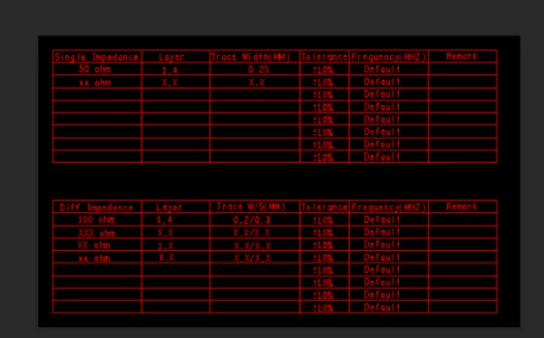
8.2 The Impedance Requirement Table
Include a table in your fabrication notes (or Readme file) with the following columns:
- Layer:(e.g., Top Layer)
- Impedance Type:(Single-Ended, Differential, Coplanar)
- Target Value:(e.g., 100Ω ±10%)
- Reference Layers:(e.g., L2 GND)
- Trace Width/Space:(e.g., 5 mil / 7 mil
8.3 Tolerance Balancing
- Standard (±10%):Sufficient for almost all consumer electronics.
- Strict (±5%~±7%):Used for military, medical, or ultra-high-speed backplanes. Note that increases cost due to the need for premium materials and lower yields.
8.4 Special Coating and Solder Mask Instructions
This is a critical, often overlooked detail. If your PCB has a large-area solder mask or specialized conformal coating, you must notify the manufacturer to perform “Post-Coating Impedance Testing.”Solder mask has a higher dielectric constant than air. When a surface microstrip is coated, the impedance typically drops by 2 to 3 Ohms.
9.FAQs
No. If your signal transition times are slow (low frequency) and your traces are short, you don’t need it. Generally, if the trace length is less than 1/10th of the signal’s wavelength, you can ignore impedance control. However, for anything above 100MHz or for high-speed protocols like USB, it is essential.
It is a historical compromise. 30 Ω provides the best power handling, while 77 Ω provides the lowest signal loss (attenuation). 50 Ω was chosen as a versatile middle ground for RF applications and has since become the default for most digital systems.
Yes. Solder mask has a higher Dk than air. When you coat a surface microstrip with solder mask, the impedance typically drops by 1 to 3 Ohms. Professional calculators have a setting to account for “Coated Microstrip.”
Yes. It is common to have 50 Ω traces for general signals and 90 Ω differential pairs for USB on the same layer. You just need to specify the different trace widths and spacings for each requirement in your fabrication notes.
The industry standard is ±10%. For extremely high-performance applications (like 28Gbps+ backplanes), you may request ±5%, but this increases the cost of manufacturing significantly as it requires more precise material selection and tighter process controls.
Yes, usually. A standard via is typically more inductive and capacitive than a flat trace. In very high-speed designs (above 5GHz), “via tuning” is required, which may include adding “anti-pads” (clearing away ground on adjacent layers) to reduce capacitance and match the via to 50 Ω.
10.Summary
PCB Impedance Control is the bridge between a theoretical circuit diagram and a functional, high-speed physical product. By managing the trace geometry, selecting the right dielectric materials, and ensuring a solid return path, you can prevent the reflections and noise that plague modern electronic designs.
When transitioning to production, always provide your manufacturer with a detailed stackup table and impedance notes. This transparency ensures that the board you receive in the mail performs exactly like the one you simulated on your screen.








