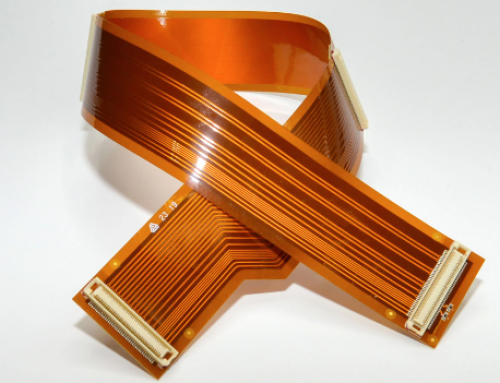
What is the PCB manufacturing process like?
This article provides a detailed introduction to the PCB manufacturing process, which is divided into 9 steps
What is the PCB manufacturing process like?
Premium quality PCB establishes minimal standards for circuit card production and setting up. It
includes three efficiency classifications based upon specifications and specs for procedure and
integrity expectations. However, for all categories, PCB manufacturing contains the adhering to steps.
Step 1, Imaging The initial step in PCB manufacturing is to produce a photo of the circuit. It is for
not just the top and lower layers of the board however also the inner layers of the stack for a
multi-layer layout. The copper layer is covered with photoresist and revealed to light.
Step 2, Etching (Inner Layers) Etching is the procedure of eliminating copper from all locations except
traces or various other conductor points. Ammonia-based remedies are normally used.
Step 3, Stacking For this action, the circuit card layers (substratum and laminate) are stacked, lined
up, and heat-pressed with each other.
Step 4, Exploration Via openings and mounting holes are pierced with these layers. It is important to
comply with the right exploration process right here and abide by element ratio restrictions.
Step 5, Etching (Outer Layers) For the outer layers, the photoresist and excess copper must be
eliminated.
Step 6, PCB Plating Drilling holes with copper plating permit present circulation between layers.
Step 7, Solder Mask A Solder mask is a polymer movie, usually environment-friendly, black, red, yellow,
or white, that protects non-conductive surface areas.
Step 8, Silk Screen Application This is where tags, polarity icons, pin one indicators, and other info
are printed on the surface of boards. These are normally used by an inkjet printer.
Step 9, Include Surface area End up The main feature of surface finish is to secure copper areas from
ecological risks, particularly wetness and oxidation.
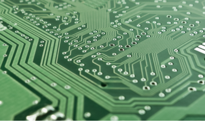
PCB processing develops the bare board or PCB with no component, which must not be confused with PCB
assembly (PCBA), where components soldering onto the board. The onset of PCBA production depend heavily
on centimeters procedures and devices. Nevertheless, the design selections you make help determine
whether your board is produced ideally.

