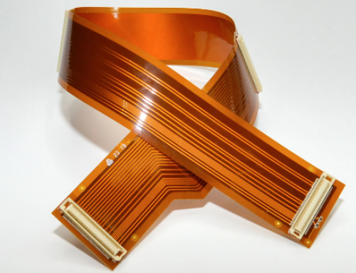
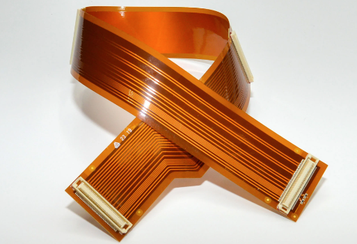
13 steps to reveal the secrets of PCB Prototyping
13 steps to reveal the secrets of PCB Prototyping, making you a PCB Prototyping expert.
13 steps to reveal the secrets of PCB Prototyping
The process of PCB Prototyping is as follows :
(1) Contact the factory: Tell the PCB factory the required size, process requirements,
product quantity, and other relevant data, wait for professionals to provide a PCB prototype quote, and place an order.
(2) Cutting: Based on the engineering information provided by the customer, cut small
pieces of production panels from the big panels that meet the requirements.
(3) Drilling: Drill holes on the plate that meet the requirements and drill the
required hole diameter at the corresponding position.

(4) Copper deposition: A thin layer of copper is deposited on the insulating hole using
chemical methods.
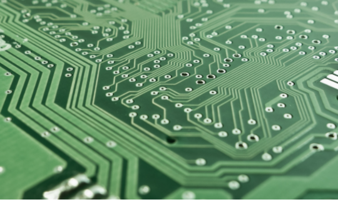
(5) Graphic transfer: Transfer the image on the production film to the board.
(6) Graphic plating: Electroplating a copper layer and a gold-nickel or tin layer of
the required thickness on the exposed copper foil of the circuit pattern or the hole wall.
(7) Stripping: Use sodium hydroxide alkaline solution to remove the anti-plating
covering film layer to expose the non-circuit copper layer.
(8) Etching: Use chemical reagents to remove non-circuit areas.
(9) Green ink: Transfer the pattern of the green ink film to the board, mainly to
protect the circuit and prevent tin from forming on the circuit when soldering parts.
(10) Characters: Some characters are printed on the circuit board for easy
identification.

(11) Gold-plated fingers: A nickel or gold layer of the required thickness is plated on
the plug fingers to make them harder and more wear-resistant.
(12) Forming: Use mold stamping or CNC machine to cut out the shape required by the
customer.
(13) Testing: Using a flying probe tester to detect defects that affect functionality,
such as open circuits and short circuits, which are not easily visible.
Summary
PCB prototyping is a significant part of the electronic product
development process. Through circuit board prototyping, we can
verify whether the circuit design is correct and evaluate the product's performance.
The quality of circuit board prototyping directly affects the quality of electronic products. Therefore,
in the process of PCB prototyping, each link needs to be strictly controlled to ensure the quality of
the PCB.

