What is the use of a PCB panel?
This article introduces what is the use of a circuit board panel(PCB panel).One-stop PCB Fabrication and Assembly from highqualitypcb.
What is the use of a PCB panel?
What is a PCB panel?
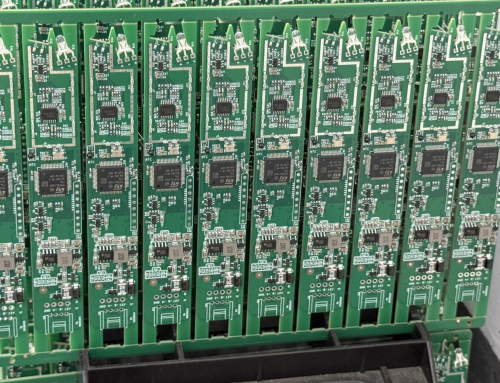
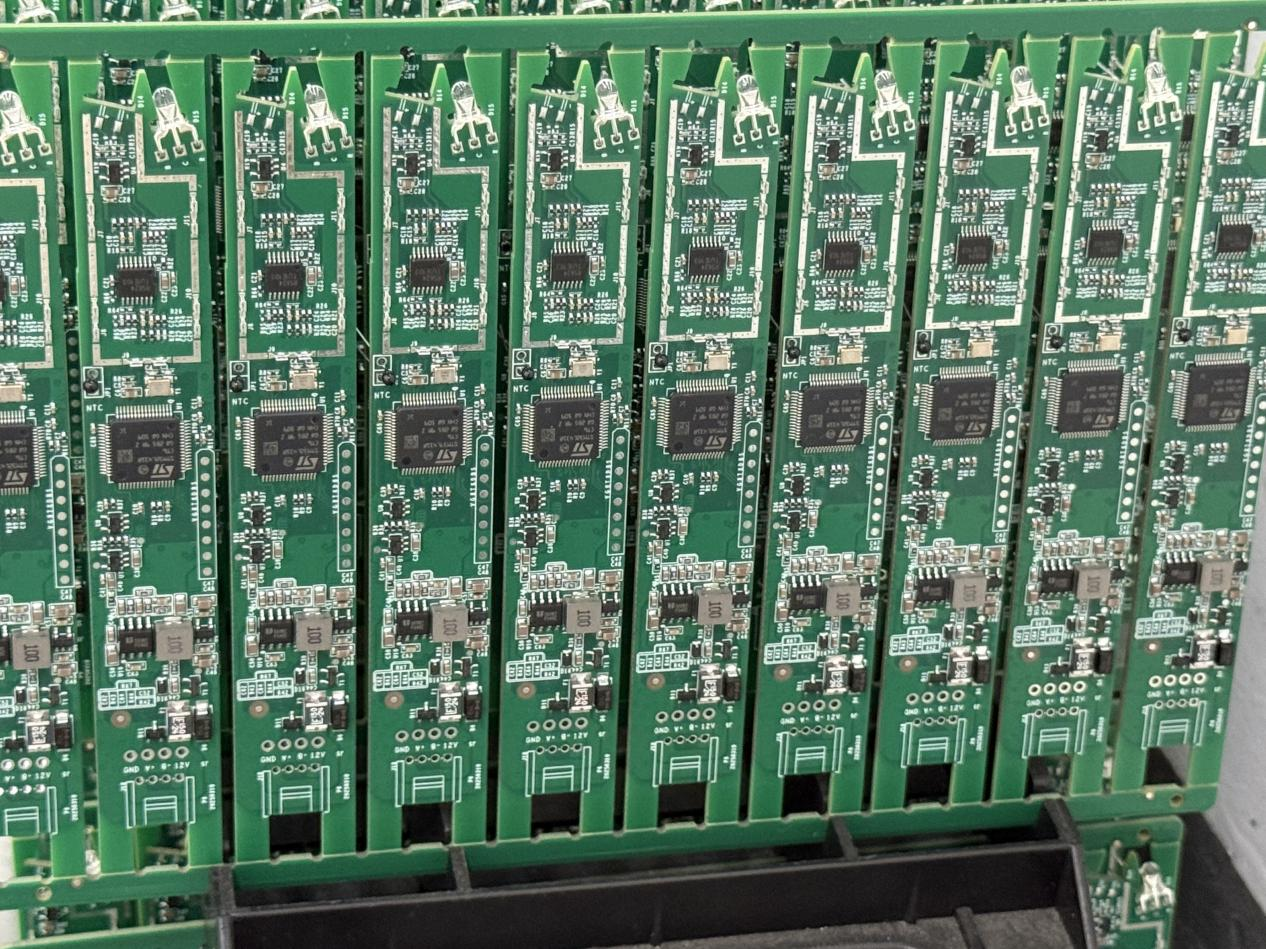
A printed circuit board panel connects two or more PCB units to form a large PCB board and has many applications and advantages.

Advantages of PCB panel
1)Improve SMT production efficiency
Processing multiple PCB units into one large PCB board simultaneously can reduce the number of board transfers and cycle frequency.
That allows more circuit board products simultaneously and improves overall production efficiency, reducing the cost of the PCB board. It is particularly significant for manufacturers that produce electronic products in high volumes.
2)Maximize board utilization
By splicing small-sized or irregular-shaped PCB units,the area of the circuit board can be fully
utilized, reducing waste and manufacturing costs. It is a critical consideration for cost-effective
production processes.
3)Reduce production difficulty
Simplifying the complex PCB structure into a simpler one can reduce the technical difficulty in the production process.
It is also critical to ensuring product quality and improving production efficiency.
PCB panel design process

During the printed circuit board panel design process, in addition to considering the fundamental
factors, you also pay attention to other details to ensure the final design product conforms to
requirements.
First, the comprehensive consideration of product characteristics needs to be more in-depth, including
accurate analysis of circuit layout, signal transmission, and power consumption.
That helps avoid complex circuit structures causing function degradation and ensures that the entire PCB
panelization system can operate stably and reliably.
In addition, board utilization and production efficiency also need to be fully optimized.
When selecting the number and method of paneling, we should consider the capacity and efficiency of the
production line to ensure that the circuit board panel plan does not introduce additional manufacturing
questions.
Excellent arrangement and design can also reduce material waste. It has a positive impact
onenvironmental protection and sustainable development.
In the product reliability and performance aspect, special needs to focus on the impact of panelization
on circuit stability and signal integrity.
A reasonable layout can avoid signal line crossover and interference. It can maintain the function of the PCB panel to the greatest extent.
The design of high-frequency circuits and sensitive components requires more accurate analysis and
layout to ensure that the product can operate stably and reliably under various working conditions.
In addition, it is also crucial to consider the processing difficulty and manufacturing cost of SMT
production.
The PCB panel plan should coordinate with the SMT
production process to avoid introducing unnecessary process difficulties.
At the same time, a comprehensive assessment of manufacturing costs, including material costs, labor
costs, and equipment costs, must ensure that the circuit board panel design is cost-effective and
feasible.
During the entire PCB panel design process, we communicate closely with the production line to ensure
that the design plan conforms to product needs and can produce productsat the same time.
PCB Panel Design + PCB Assembly Under One
Roof
Summary
In a word, printed circuit board panel design is a complex and comprehensive process. It requires engineers to consider comprehensively at different levels.
Careful design can improve production efficiency, reduce costs, and ensure that products reach optimal reliability and performance.
Today, as technology and manufacturing continue to advance, the optimized design of PCB panels will play
an important role in promoting electronic product manufacturing to a higher level.

