Welding bridging issues during PCBA processing
This article takes a deep look at the defects that affect SMT yield during the printing process and finds their root causes.
Welding bridging issues during PCBA processing
As the size of electronic products continues to shrink year after year, printed circuit board assembly (PCBA) manufacturers are facing a new set
of major challenges. The trend towards more miniaturized and compact electronic products will certainly
continue. Smart PCBA manufacturers are actively addressing these challenges to adapt to these changes
and prepare for future developments. One major obstacle that everyone in our industry must overcome is
the problem of welding bridging.
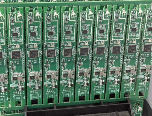
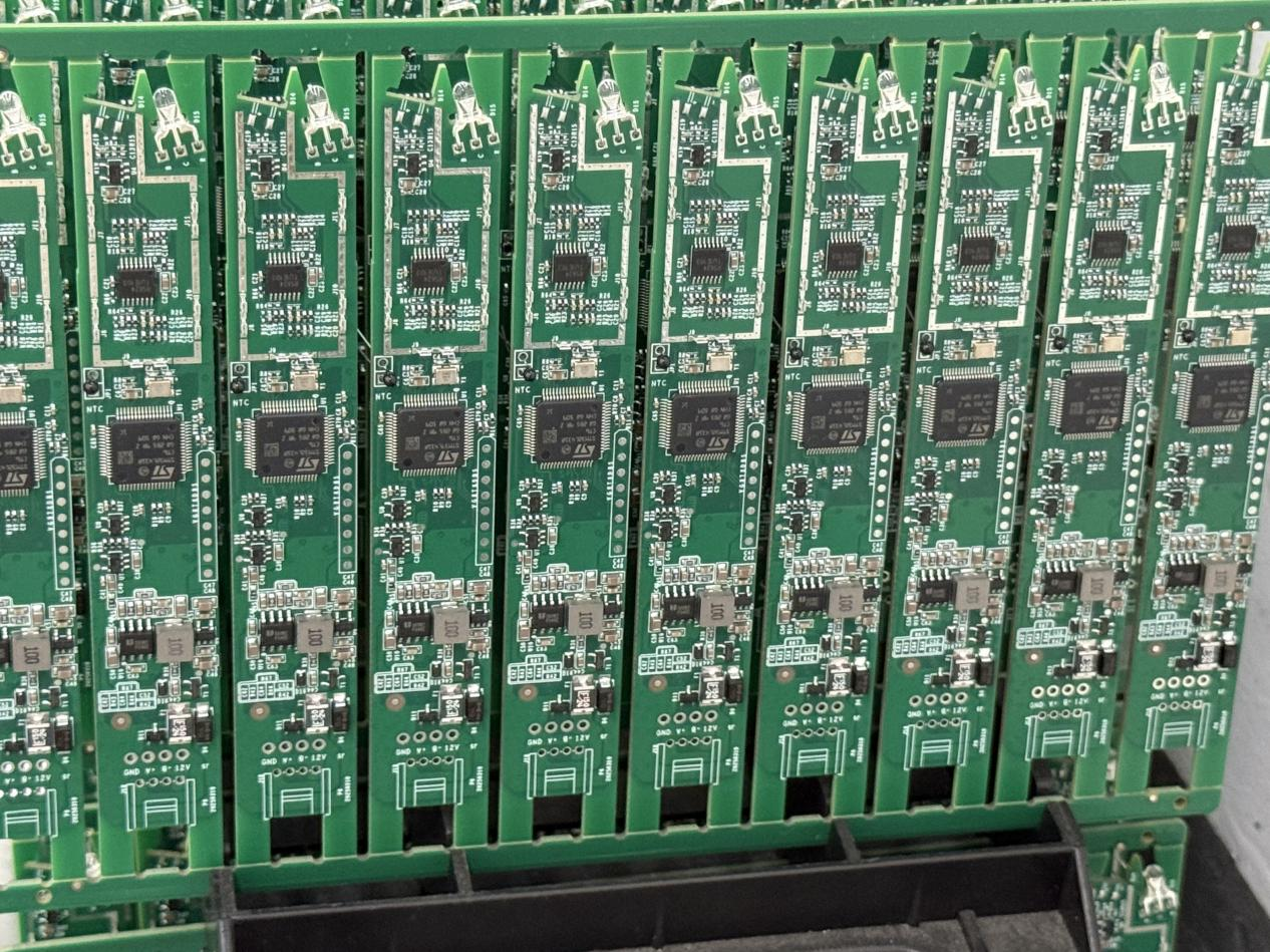
Welding bridging is a common defect in surface mount technology (SMT). This occurs when
welding flows between connectors and causes a "bridge" or short circuit. When welding bridging
occurs, it is not always immediately obvious…but it can cause serious damage to electronic components
or devices. Bridging can occur at multiple points in the manufacturing process. Sometimes, it can occur
during the welding paste printing, which is caused by welding paste being squeezed between the printed circuit board (PCB) and the steel mesh and depositing additional
welding paste. It can also be caused by factors such as PCB manufacturing problems, pressure when
placing electronic components, improper settings of the reflow oven, etc. Bridging is caused by board
design problems, too much paste, or other problems, and it is undoubtedly a headache for PCBA
manufacturers.
Methods to reduce welding bridging
To reduce welding bridging, we must recognize that there is no single, reliable method
to eliminate it, as welding bridging is caused by a variety of factors. However, we have researched and
found ways to reduce bridging and would like to share some best practice strategies with you.
(1) Adjust board design
This is not always possible. Contract PCBA manufacturers do not always have a say in optimizing board
design. However, when possible, it is one of the most effective ways to reduce bridging, especially by
adjusting the aperture width and area ratio. In addition, welding mask barriers can be added between
fine pitch pads to prevent welding bridging. welding mask-defined pads can also prevent bridging,
especially in areas with narrow pitches, such as BGAs and LGAs.
(2) Adjust the reflow profile
Increasing the dwell time above the liquidus will give the welding more time to flow to where it is
supposed to go. Once the pad and lead reach the same temperature, the welding will wet both, prompting
the welding to move to the intended location. Liquid welding tends to flow to the hotter surface first.
Due to the lower thermal mass of the electronic component leads and the increased airflow around the
leads, they may run hotter than the welding pads. Increasing the soak time will even out the temperature
across the electronic component and reduce the tendency of welding to flow to hotter surfaces.

(3) Reduce the risk of non-contact welding paste printing
Try adjusting the stencil design to reduce the amount of welding paste in the problem area. You can also
adjust the board design to eliminate factors that cause poor printed contact. Legend marking ink next to
the pads defined by the welding mask can cause a few mils of debonding, which can significantly increase
the amount of welding paste.
(4) Reduce the amount of welding paste or component lead size
Bridging can be significantly reduced by modifying the SMT stencil to reduce the volume or location of
welding paste on the pad. After all, bridging problems can occur when welding reaches places it
shouldn't.
Assemblies with increased lead size can also reduce the possibility of welding flowing between leads.
Increasing the size of the component helps to occupy more welding, thereby preventing it from
overflowing between pads. A common cause of welding bridging is that the pad design is for long leads,
while the alternative component assembly has shorter leads. The welding must wet a relatively large area
on the pad, reducing the volume that can flow along the lead.
Thermal differences are particularly challenging for gull-wing leads. During the reflow welding process,
welding paste can pool and cause bridging. Try adjusting the stencil to reduce the amount of welding
paste printed on the pad.
Engineering Support
Experiencing bridging issues? Need help to solve welding problems?
More resources to help avoid welding bridges SMT defects
Need more help? These technical papers from our field application engineers provide more insights and
guidance on solving issues that reduce SMT PCBA processing yields, including bridging.
Using root cause analysis in stencil design to improve PCBA processing yields, PCBA manufacturers can
save cost and time and improve product reliability by reducing first-pass defects. Yield can be
summarized as cost, delivery, and reliability, which are the key elements to achieving effective and
profitable PCBA processing.
welding paste printing is the main cause of yield issues for PCBA manufacturers… and this phenomenon
is getting worse with the trend toward smaller form factors.
Highqualitypcb SMT: This article takes a deep look at the defects that affect SMT yield
during the printing process and finds their root causes. Additionally, it investigated how the weight
and surface treatment of the outer copper layer affected printability.

