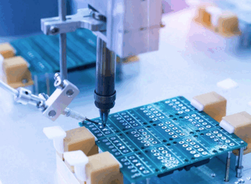
A Step-by-step Guide to PCB Assembly Testing & Inspection
PCBA testing is more than just finding defects. It is a quality driver for the entire value chain. From start to finish, it covers design validation and process control.

PCB assembly testing methods are essential to the manufacturing process.
We are constantly adjusting and improving our testing methods alongside failure analysis. We will describe in detail the various PCB test methods. This guide is intended to provide a concise and informative compilation of these insights.
1.Incoming Quality Control
(1)Purpose: PCB assembly materials include PCB substrates and electronic components.
Verify that the materials used meet all performance, specification, and reliability requirements.
(2)Inspection Content:
You can detect some issues in advance by inspecting the incoming materials.
You must check the packaging and silkscreen of the component before assembly. You need to inform the supplier if the pins of the component oxidize and order replacements in time.
You must verify that the electrical parameters of the components meet the standard before assembly.
You should check the pad flatness and thickness of the PCB before PCB assembly. Check the surface coating and via quality.
2.Stencil Inspection
(1)Purpose: Ensure the stencil remains clean. Confirm that SMT stencil tension and aperture precision meet specified process parameters.
(2)Inspection Content:
Confirm stencil aperture dimensions follow design-specified process requirements. Tests include shape, aperture size, and placement tolerance.
Make sure the stencil is clean and free from contaminants or solder paste residue.
Check stencil tension with a tensiometer for consistent printing.
3.Solder Paste Inspection (SPI)
(1)Purpose: The goal of SPI is to inspect solder paste printing quality. It also prevents soldering defects like excessive/insufficient solder, bridging, and misalignment.
(2)Inspection Content:
Check that the paste volume and the thickness correspond to the specifications. Position the solder correctly. The solder paste shape should also match the print specifications.
You need to fix the misaligned solder paste as soon as possible.
Also, you need to check the edge clarity as well as the presence of bridging.
incoming quality control, stencil inspection and solder paste inspection
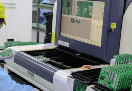
4.In-Line Automated Optical Inspection (In-Line AOI)
(1)Purpose: After reflow soldering, surface mount defects can be identified immediately. This allows for immediate feedback on the process. AOI inspects PCBs using 2D or 3-D cameras. The board is not powered and some components are missing.
(2)Inspection Content:
You can detect misplaced or missing components immediately with in-line AOI. This is also useful for checking component polarity, skewing and tombstoning.
You can detect defects early by using in-line AOI. You can immediately rework defects such as bridging and pad contamination.
AOI systems detect other defects using machine vision and cameras. Open circuits, pad damage, and lead deformation can all be detected quickly. It helps reduce the errors and costs that come with PCBs that are faulty.
5.SMT First Article Inspection (FAI)
(1)Purpose: Test the first assembled PCB before full production. Make sure the process is correct to avoid batch mistakes.
(2)Inspection Content:
Verify the BOM for the correct model of the component mounted. The component package must also be examined, as well as the polarity.
In addition to X/Y offset, the rotation angle is also included in the placement accuracy. The machine should be debugged if the accuracy is incorrect.
You must ensure that the pads and leads are coplanar for QFP and BGA parts. It’s very easy to find soldering faults if you don’t.
6.Reflow Profile Monitoring
(1)Purpose: Verify the reflow oven has the right temperature curve. It must match the needs of the solder paste and components. It can be used to prevent defects like cold soldering or pad detachment.
(2)Inspection Content:
The temperature curve is primarily concerned with the peak temperature and heating rate. Correcting incorrect cooling rate and holding times should be done in time.
The thermocouple plates can be used to detect temperature differences between areas.
in-line automated optical inspection, smt first article inspection and reflow profile monitoring
7.In-Process Quality Control
(1)Purpose: It’s important to perform real-time sampling when assembling PCBs.
It is important to check critical processes, such as reflow parameters and mounting conditions. Early detection and correction of defects is important in the PCBA manufacturing process.
(2)Inspection Content:
You can then determine the scope of the batch sampling based on the different shifts.
Verify process parameters such as solder paste thickness.
You must ensure that the production environment is correct. Temperature and humidity must be appropriate. ESD protection must also be present.
8.In-Circuit Test (ICT)
(1)Purpose:
Use bed-of-nails or flying probe systems to test circuit connectivity. This tool is used to find open circuits, component values, and shorts. The system is designed to cover 100% of the components, but in reality, it covers 85-90%. (There are no human errors). ICT focuses on large connectors and BGAs.
(2)Inspection Content:
Verify that resistance values are not normal.
You should also check the function pin connections of diodes, transistors, and other components.
You can correct a circuit network that is short or open in a timely manner.
9.Functional Test (FCT)
(1)Purpose: Verify that the assembled PCB performs as intended. This test verifies that the board is performing as intended.
(2)Inspection Content:
Power up the board during this inspection. Send input signals and check if outputs match specs. Unlike component tests, this evaluates full PCBA performance under real-world conditions.
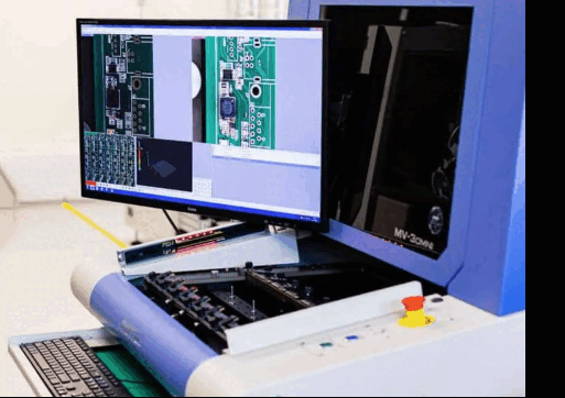
10.Offline Automated Optic Inspection (Offline AOI)
(1)Purpose: Inspect high-density complex structures. This is a complementary tool for in-line AOI.
(2)Inspection Content:
It uses the same principles as inline AOI but in a slightly different order. This complements in-line AOI by focusing on hard-to-reach spots like BGA peripheral pads.
in-process quality control, in-circuit test, functional test and offline automated optic inspection
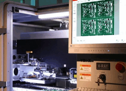
11.X-ray Inspection
(1)Purpose: X-ray is available in 3D and 2D. The 3D version is faster. This method is used to detect defects in solder joints that are not visible, such as BGA bottom joint. This method is effective but requires skilled operators.
(2)Inspection Content:
This inspection allows you to check the condition of both the solder points and the solder. It’s important to check for cracks in solder joints and other problems with soldering.
Tests for solder ball coplanarity are required. It is also necessary to test the connection integrity and connection strength.
Correct the problem immediately if the bottom of the component is not aligned to the PCB pads.
12.Wave Soldering Inspection
(1)Purpose: After wave soldering, inspecting through-hole joint quality is crucial.
(2)Inspection Content:
This is also a good way to check the appearance of solder joints. Rework immediately if any of the gloss, icicles or saturation is wrong.
This is to test via solder penetration. Rework it immediately if the solder penetration is poor.
Replace any components damaged by heat as soon as you find them.
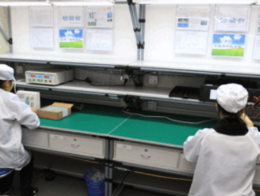
13.Manual Visual Inspection (MVI)
(1)Purpose: This inspection adds to automated tests. It helps judge irregular or complex defects qualitatively.
(2)Inspection Content:
Look for any cosmetic flaws, such as a distorted silkscreen. Contact the assembly factory to fix this as soon as you can.
Rework the joint if it is not wettable or glossy enough. Clean PCBs with flux residue after assembly.
You should act quickly if the connector/cable does not feel firm when you inspect it.
x-ray inspection, wave soldering inspection and manual visual inspection
14.Reliability Testing
(1)Purpose: Regularly check how PCBA performs stably under harsh conditions. This is highly essential for military and automotive electronics.
(2)Inspection Content:
Reliability tests cover environmental stress tests, mechanical stress tests, and burn-in tests.
These tests simulate extreme conditions that a PCB may face during its lifetime. Extreme conditions include high temperatures, high voltage, and mechanical strain. Humidity, bend strength, and vibration are external environmental factors. This lets engineers confirm performance and reliability to meet specifications.
15.Final Quality Control (FQC).
(1)Purpose: Final QC thoroughly inspects the completed PCBA. Test the assembled PCB to ensure it meets customer specs and requirements.
(2)Inspection Content:
Randomly sample X-rays and AOIs according to the different product categories.
You can perform functional retesting by focusing on the features specific to your customers.
You should also pay attention to the packaging and labeling during this test.
16.Quality Assurance Shipment Inspection
(1)Purpose: Before shipping, you need to confirm the quality of the assembled PCB. Stop defective products from reaching the customer.
(2)Inspection Content:
Check the packaging, functionality, and appearance of samples using standards like MIL-STD-105E. Review shipping paperwork such as compliance certificates, test reports, and traceability logs.
Test the package for shock resistance and compression.
reliability testing, final quality control and quality assurance shipment inspection
17.Possible Problems And Solutions during PCBA Testing
17.1 Incoming Quality Control
| Common Issues | Solutions |
| Resistance/capacitance values out of tolerance; IC models not matching BOM. | Implement intelligent barcode scanning to auto-match BOM data with component labels. Integrated with RoHS compliance database. |
| Contaminated PCB pads, Oxidized component leads, blurred silk screening. | Use automated optical measuring instruments (AOI) to inspect pad flatness and lead coplanarity. |
| QFP package dimensions mismatched with PCB pads; reversed diode polarity. | Apply visual positioning systems for polar components to auto-identify orientation, reducing misjudgment rates. |
17.2 Stencil Inspection
| Common Issues | Solutions |
| Insufficient solder paste due to reduced openings. | Use 3D laser scanners for measuring stencil apertures. |
| The tension will be below the rated value if you use it excessively. This can compromise printing precision. | Create a stencil lifecycle management system. Replace stencils at a specific value tension using automatic calibrators. |
| Dry solder paste can clog up the apertures and cause printing to leak. | Ultrasonic cleaning + ionized dry air. Manually sampled apertures using a 10x magnifier. |
17.3 Solder Paste Inspection (SPI)
| Common Issues | Solutions |
| Edge thickness can vary due to scraper pressure instability. | Closed-loop pressure control systems can be installed with a pressure sensor and servo motor. |
| Misalignment of PCBs due to worn-out PCB locator pins. | Use real-time positioning of PCBs with vision alignment systems. |
| Solder paste adhesion between fine-pitch pads. | Apply stepped stencils and edge anti-squeeze design for fine-pitch components. SPI 3D measurement corrected. |
17.4 First article inspection (FAI)
| Common Issues | Solutions |
| The capacitor was misapplied to a resistor. BOM updates were not synced. | Use an AI-based visual FAI System. Compare component shapes, silkscreens, and BOMs automatically. Calculate the component recognition rate. |
| The pick-and-place vision is not correct. This leads to the incorrect orientation of electrolytic capacitors. | Dual-light imaging (red + Blue) is used to detect polar components. Machine learning can be used to detect polarity. |
| Solder joint openings due to QFP warpage. | Introduce coplanarity laser detectors for lead scanning. Automatic line stops are triggered for results that are out of tolerance. |
17.5 Incoming Quality Control
| Common Issues | Solutions |
| Faulty thermocouples can cause a peak temperature of >250°C (lead-free limit). | Equip multichannel temperature testers to collect curves every 2 hours. Automatically alarm when the limit is exceeded. |
| Increased temperature variations within the board are caused by an uneven hot air motor speed. | Weekly dynamic balance tests are recommended to calibrate the hot air motors. Test temperature uniformity using temperature test boards. |
| Leaks in the cooling system can cause it to cool faster than specified, causing cracks. | Use nitrogen reflow for soldering. Control cooling fan speed using the PID algorithm. |
17.6 Inline AOI Inspection
| Common Issues | Solutions |
| Low contrast can cause invisible bridging at small solder joints. | Multi-angle lighting (0deg/45deg/90deg), paired with 3D AoI, will enhance contrast and height analysis. |
| False positives due to component color variation. | Create component feature databases that have independent detection thresholds for colors and materials. |
| BGA shadows can obscure the detection of adjacent capacitor solder joints. | Install tilted cameras (15deg angle) for BGA peripherals. AI image segmentation can be used to identify occluded joints. |
17.7 In-Circuit Test (ICT)
| Common Issues | Solutions |
| Probe wear causes false open circuit judgment (contact resistance > 50mΩ). | Replace worn probes with spring pressure sensors. |
| PCB warpage leads to uneven probe pressure. | Introduce auto-leveling fixtures and laser profilers to compensate for warpage in real-time. |
| Parameter deviations are caused by the temperature-affected ESR in electrolytic capacitors. | To minimize thermal effects, precondition the PCBA before testing at a constant temperature. |
17.8 Functional test (FCT)
| Common Issues | Solutions |
| Signal interruptions can be caused by oxidized connector pins. | Apply moisture-resistant coatings + gold-plated connectors with automatic pin cleaning. |
| Incorrect firmware and testing programs can lead to a misjudgment. | Set up firmware version management systems to automatically verify compatibility. |
| Undetected functional failures when input voltage exceeds the rated +-10%. | Simulate wide voltage inputs (+-20%) using a programmable power supply (high accuracy). |
17. 9 X-ray Inspection
| Common Issues | Solutions |
| BGA solder joint voids >20% area can impact reliability. | Use low-void pastes (voids less than 10%) and optimize reflow profiles. |
| Low-resolution images can miss the invisible inner-layer delamination. | Upgrade to computed tomography with microfocus X-ray system for delamination identification. |
| The small solder joints are difficult to evaluate due to blurred details. | Create solder joint defect databases using deep learning to auto-identify internal issues. |
17.10 Reliability testing
| Common Issues | Solutions |
| After 500 cycles at -40~85, cracks in the solder joint are visible. | Use underfill to improve fatigue resistance. |
| Loose connector contacts can cause intermittent shorts. | Use pre-vibration force testing and screw torque monitoring systems (>5N). |
| Pad rust is caused by an inadequate conformal coating. | Use nano-coating to increase salt fog resistance up to 1,000 hours. |
18.PCBA Testing: Top Practices
PCBA testing is a key component in ensuring product quality, reliability, and functionality. The following are key strategies for optimizing testing:
18.1 Ongoing optimization
Analyze data and test strategies regularly. It is able to adapt well to changing technologies and requirements.
18.2 Testability design
Plan PCBs to have a large number of test points. Leave enough space around the PCBs for access to probes and other equipment.
18.3 Documentation and Feedback
Document all test results, defects, and procedures. Create clear feedback loops for the design, assembly, and testing teams. It promotes continuous improvement and early problem resolution.
18.4 Process Control and Quality Assurance
Verify operational durability by following standard test protocols and performing environmental tests.
19.PCBA Testing Challenges
PCBA testing is hampered by:
19.1 Software and Hardware Integration
Integration of multiple hardware and software tools is often required for testing. It is a challenge to ensure seamless compatibility among these systems.
19.2 Cost and time constraints
The cost of high-quality tools such as X-ray and ATE systems is expensive. Some tests can also cause production delays.
19.3 Signal Integrity and Risks
Noise, reflection, and crosstalk can cause input signals to weaken or be distorted. Signal integrity is important when assembling PCBs.
19.4 Accessibility and Coverage
During PCB design, it is difficult to include comprehensive test points and functionality. This also limits the full coverage of tests.
19.5 Dense Component Layouts
Modern PCBs are made up of miniature components that have a tighter spacing. Visual inspection is impossible, and the test points are difficult to reach.
20.Summary
Testing methods for PCB assembly—such as visual inspection, X-ray testing, in-circuit testing, and functional testing—are vital for component performance. They help detect flaws and ensure adherence to design and industry standards. Thorough testing reduces failures and recall costs, enhancing customer trust. Complex electronics require increasingly sophisticated testing techniques.
Looking for a PCBA professional partner? Orinew provides turnkey PCBA solutions that include everything from design and manufacturing to component sourcing. Visit our website or contact us online to find out more.

