7 Common PCB Assembly Challenges And Solutions
As a cornerstone of the electronics industry, understanding fundamental PCB Assembly issues and their solutions is vital for PCB assembly professionals.

PCB assembly is at the heart of modern electronics. PCBs play a vital role in the reliability and functionality of electronic devices. The complexity of assembling these boards may present a number of challenges. If not addressed, this can result in costly mistakes and product failures. Whether you are a professional in the field or a beginner, you should know PCBA challenges.
This blog is intended to help you navigate through common problems. These problems occur during PCB assembly. It also provides practical solutions for ensuring your assemblies are reliable and efficient.
There are totally seven kinds of issues about common problems and related solutions to PCB assembly.
1.Component Issues
1.1 Physical Damage
Components are damaged due to improper handling or transportation. This includes cracks, bent pins, missing pads, or cracked packages.
Solution:
We should package components well and avoid collisions during transportation.
1.2 Oxidation/Corrosion
Leads lose their gloss or become wet, causing surface contamination. This affects the solderability of the component.
Solution:
We should focus on preventing moisture and contaminants from reaching the leads and using protective coatings.
1.3 Counterfeit Parts
Components are substandard or counterfeit. They can usually be detected by XRF material analysis or chip photography.
Solution:
We should cooperate with trusted suppliers. You can always trust Orinew that our components are 100% genuine.
1.4 Polarity/Orientation Errors
Electrolytic capacitors are not marked with polarity. Diodes are marked with reverse polarity. IC pin indications are misaligned. These can lead to functional failures after soldering.
Solution:
We need to remove and replace these faulty components in time to avoid functional failures later.
1.5 Component Floating/Tilting
The insertion is insecure. The holding force is insufficient during soldering. Or the buoyancy is excessive from the wave. They can lead to misaligned components, incorrect lead immersion, and failed solder joints.
Solution:
Do a good job of employee training to ensure proper operation. Maintain routine inspections and commissioning of machines to ensure accurate machine operation.
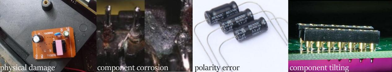
Component Issues of physical damage, component corrosion, polarity error, and component tilting;
1.6 Material Composition Errors
Substrates are non-compliant or plating is incorrect.
Solution:
Always use qualified substrates and adopt the correct plating method.
1.7 Component Missing/Excessive Placement
Feeder and programming errors can bring missing components or duplicate placement. This results in functional failures or shorts from duplicates.
Solution:
Perform manual or automated checks of the first assembled board. Confirm all components are present and correctly placed, catching feeder misalignments early. Perform routine inspections and replace worn parts promptly. Use calibration fixtures to ensure feeders dispense components at precise intervals and angles.
2.Design Issues
2.1 Footprint Mismatch
SMD component size or pin spacing is inconsistent with Gerber/BOM.
Solution:
Before finalizing the design, cross-check component footprints with the Bill of Materials (BOM). Use design rule check (DRC) tools. Flag mismatches in pad spacing, pin orientation, or package size. Conduct a DFM review with the assembly team to validate footprints.
2.2 Poor Thermal Management
PCB assemblies produce heat during operation. When thermal management is insufficient, overheating can occur, potentially damaging sensitive components.
Solution:
To address this, designers should integrate heat sinks, thermal vias, or cooling fans into the layout. Selecting materials with high thermal conductivity also helps efficiently dissipate heat and maintain optimal operating temperatures.
2.3 Pad/Hole Design Flaws Too Small Pads
Inadequate solder adhesion and mechanical strength.
Pad/Hole Design Flaws Too Small Pads
Incorrect Hole Diameter: Poor lead fit (too tight/loose), leading to solder voids or pull-out.
Uneven Pad Layout: Asymmetrical heat dissipation causing soldering inconsistencies.
Solution:
Avoid placing vias under BGA, QFN, or fine-pitch components. They complicate rework and increase short risks. Use blind/buried vias for internal layers if needed. Base solder pad dimensions (length, width, thickness) on component datasheets and IPC-2221 guidelines. Ensure minimum annular ring sizes based on board thickness and drill tolerance.
3.Functional Issues
3.1 Parameter Deviation
Out-of-tolerance values or unstable performance.
Solution:
Source components from authorized distributors with traceability (e.g., ISO 9001-certified). Perform 100% automated optical inspection (AOI) of passive components for physical damage.
Parameter Deviation
3.2 Open/Short Circuits
Faulty connections in multi-lead components or intermittent failures in connectors with poor contact resistance.
Solution:
Use pad spacing compliant with IPC-7351. Avoid placing vias under BGA pads to minimize shorts from misaligned reflow. Use no-clean flux with low ionic residue to prevent dendritic growth over time. Use low-temperature solder to avoid overheating leads and causing opens.
4.Environmental Issues
4.1 Adhesive Failure
Low post-cure bond strength or substandard Tg.
Solution:
Choose adhesives with Tg ≥20°C above the maximum operational temperature. Remove oils, oxides, and mold release agents. Adhesives need clean, roughened surfaces to bond properly. Inadequate curing time or temperature can lead to low bond strength and low Tg. Use time-temperature integrators (TTIs) to track cumulative cure exposure.
4.2 Cleaning Agent Residue
Ionic contamination exceeding IPC-5701 limits.
Solution:
Choose different cleaning agents according to different types of contaminants. Source cleaners are compliant with IPC-8010 (aqueous cleaning) or IPC-CC-830 (solvent cleaning). Use automated optical inspection (AOI) to map flux distribution post-reflow. Flag boards with excessive bridging or non-uniform flux coverage for extended cleaning.
4.3 Humidity and Moisture
The ambient humidity is too high. Or PCB storage is unprotected. It can lead to pad/pin oxidation or flux failure. It can also cause poor wetting, increased voiding, or flux splashing during soldering. The QFN and BGA components are not properly dry-packed. This can cause delamination or “popcorning” during reflow soldering due to moisture absorption.
Solution:
Store PCBs and components in moisture barrier bags (MBBs). We should be equipped with desiccant packs, humidity indicator cards (HICs), and seal bags. Use dry cabinets or climate-controlled vaults for MSCs awaiting assembly. Bake components (per JEDEC J-STD-033) if exposure exceeds floor life. Use aluminum foil laminate bags with heat-sealed edges to store components. Apply UV-curable acrylic or silicone coatings to seal against post-assembly moisture ingress.
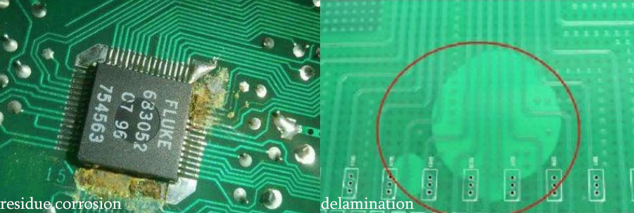
Environmental Issues of residue corrosion, delamination
5. Soldering Process Issues
5.1 Tombstoning (Component Lifting)
Uneven pad heat due to asymmetric thermal mass.
Solder paste volume is imbalanced or component placement misaligns.
Solutions:
Use symmetrical pad layouts with matched thermal reliefs.
Select high-activity solder paste (e.g., SAC305) to improve wetting.
5.2 Solder Balling
Moisture in solder paste or PCB substrate vaporizes during reflow.
Excessive solder paste deposition or rapid temperature spikes cause splatter.
Solutions:
Bake PCBs pre-assembly if humidity is higher than a certain value.
Add solder mask dams between pads to contain paste. This prevents solder paste deposition.
5.3 Solder Bridging
Stencil misalignment or oversized apertures deposit excess paste.
Low-viscosity solder paste spreads during reflow.
Solutions:
Deploy SPI (Solder Paste Inspection) pre-reflow to flag paste volume deviations.
Adjust wave soldering conveyor angle for optimal separation.
5.4 Cold Solder Joints
Heat insufficiently during reflow or pads contaminate.
Component lead oxidation impairs wetting.
Solutions:
Extend soak zone duration in the reflow profile to ensure full melting.
Use plasma cleaning of pads to remove oxides before assembly.
5.5 Voiding in BGA/CSP Joints
Flux gases or moisture traps in microvias.
Hole fill is poor during PCB fabrication.
Solutions:
We can use vacuum reflow ovens to reduce voids.
We can also mandate X-ray checks per IPC-7095 for 100% BGA coverage.
5.6 Head-in-Pillow (HIP)
BGA ball/pad oxidates or PCB warpages during reflow.
Temperature is inadequate to fully melt solder spheres.
Solutions:
We should store BGAs in moisture-proof bags and pre-bake them.
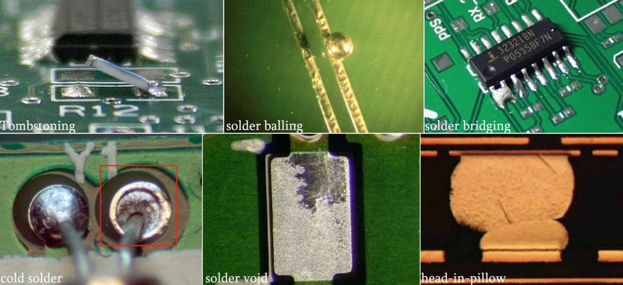
Soldering Process Issues of tombstoningj, solder balling, solder bridging, cold solder, solder void, pillow
5.7 Wave Soldering Defects (Blowholes, Icicles)
Moisture exists in through-holes or conveyor angles is incorrect.
Solutions:
We can pre-bake PCBs to eliminate moisture.
And we can also optimize wave nozzle pressure and flux spray uniformity.
5.8 Pad Leaning/Tilting
Inadequate vacuum pressure can cause component lift from the PCB surface. Partial pad contact makes semi-wetted joints with reduced vibration resistance. This is prone to fatigue cracking over time.
Solution:
Optimize vacuum pressure in placement equipment. Ensure it’s sufficient to hold the component securely. Flatten warped PCBs using thermal reconditioning or vacuum chucks. Check component coplanarity. Reject bent leads or warped bodies from suppliers. Train staff on nozzle selection, vacuum troubleshooting, and recognizing tilt signs. Implement In-Process Inspection in time to catch drift early.
5.9 Incorrect Component Orientation/Position
Human error appears during insertion. Jigs misalign, or assembly drawings are unclear. These will lead to misplaced leads and mistaken soldering.
Solution:
Strengthen employee training on standardized operations.
5.10 Irregular Solder Joints
Oxidized or uncleaned iron tip, reducing solder fluidity. Premature flux volatilization or rapid air movement can cause irregular solder joints. Insufficient mechanical strength is prone to stress fracture. Sharp spikes risk high-voltage arcing or short circuits.
Solution:
Regularly clean and tin the iron tips. Replace them promptly based on usage. Choose the right flux. Limit soldering time per joint to keep flux active. Refine the soldering technique, and ensure proper hand placement and motion. Use high-quality solder paste to avoid spattering or voids.
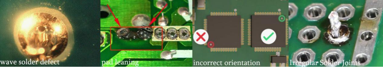
Soldering Process Issues of wave solder defect, pad leaning, incorrect orientation, irregular Solder Joints
5.11 Lead Deformation/Breakage
The insertion force is excessive. The lead forming is improper. Or there is mechanical stress from the wave impact. They can cause damaged leads, open circuits, or difficulty in subsequent rework.
Solution:
Implement precision automated machines with force sensors to control insertion force. Enforce gentle handling for manual insertion. Use vacuum pickup tools or tweezers to avoid direct pressure on leads. Optimize Wave Parameters, and use pins, or clamps to secure the PCB. Align leads parallel to the wave flow to minimize lateral stress.
5.12 Component Corrosion
Acidic cleaners can erode metallic coatings. Alkaline cleaners discolor pure tin/silver immersion coatings. Contact resistance increases when connector pins are corroded. Signal transmission problems can occur. The corrosion of nickel pads reduces the adhesion between solder joints. This results in cold solder.
Solution:
Use pH-neutral or specialized electronics cleaners. This avoids attacking metallic coatings. Validate cleaning agents against the specific surface finishes. This prevents corrosion and maintains reliability.
5.13 Mechanical Stress
Over-spray pressure can displace components. Electrolytic capacitors can be damaged by an incorrect ultrasonic frequency. QFP lead is deformed by cleaning fluid impact. BGA ball micro-cracks appear due to vibration stress.
Solution:
Control spray pressure to prevent component displacement. Avoid Ultrasonic Damage to Electrolytic Capacitors. Prevent QFP lead deformation from fluid impact. Use vibration-dampening fixtures, avoid rough handling, and mitigate vibration-induced BGA micro-cracking.
Soldering Process Issues of lead deformation, component corrosion, mechanical stress
6.Testing Issues
6.1 Functional Testing Failure
A frequent challenge in PCB testing is insufficient testing scope. We may neglect or shortcut test procedures. This often leads to undetected errors in the final production stages. Failing to account for product-specific testing environments can also compromise PCB performance. Environmental factors include humidity levels, temperature fluctuations, and mechanical vibrations. They directly impact product quality and its ability to withstand real-world conditions.
Solution:
PCB manufacturers verify the assembly process through circuit board testing. This ensures each component pin properly connects to its corresponding circuit net. To conduct comprehensive tests, test points must be strategically placed. They should follow Design for Test (DFT) guidelines. Without complete test point coverage, manual validation becomes necessary to address untested connections.
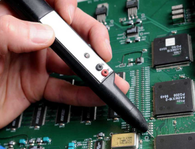
6.2 Flying Probe Testing
Probes oxidize brings higher contact resistance and misjudging opens.
Solution Pay attention to routine inspection and replace the oxidation probe in time.
6.3 ICT (In-Circuit Test)
The fixture bed-of-nails is inaccurate. It risks short circuits. Spring pins age leading to insufficient force. It causes unstable contact and intermittent misjudgment.
Solution:
Timely debug the accuracy of the fixture needle bed and replace new spring pins.
testing failure
7.Packaging Issues
7.1 Damaged Reels/Rays
Reels and trays are damaged. It is bad for transmitting.
Solution:
Use ESD-safe plastic reel trays with built-in foam inserts during transit. Use robotic arms with vacuum grippers to load/unload reels, reducing manual mishandling.
7.2 False Packaging
Anti-ESD packaging is improper for sensitive devices.
Solution:
Ban non-ESD materials from direct contact with components. Ensure bags are heat-sealed with conductive tape (not plastic clips) to create a Faraday cage effect. Add humidity indicator cards (HIC) for moisture-sensitive devices.
8. Summary
PCBA problems are mainly caused by process deviations, incompatibility of materials, instability of equipment, and human errors. Standardized operations, statistical process control (SPC), first-article inspections (FAI), and automated tests (AOI/X-ray) are required to mitigate.

