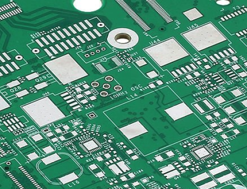
What are the advantages of using blind and buried vias in PCB?
Highqualitypcb has been in the PCB space for 15 years and offers several services and technologies to help make your life easier.
What are the advantages of using blind and buried vias in PCB?
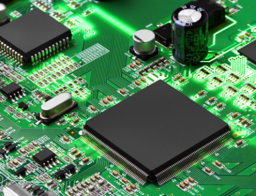
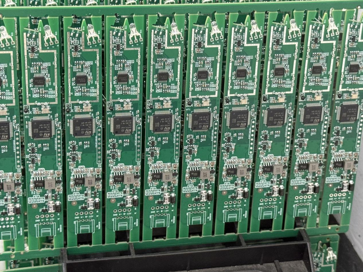
PCBs tend to be crowded, and connecting the required components to both sides of the board can become
difficult. Often, the best way to get the space you need is to use blind and buried vias to get all the
appropriate elements onto the PCB board. Of course, many people aren't entirely sure what blind and
buried vias are or how to use them. It's important to understand what they are and how they can
help.
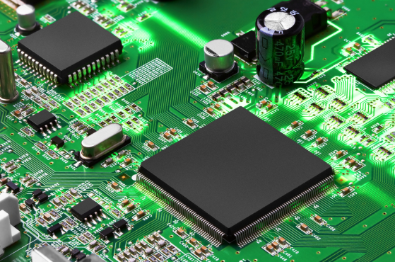
What is a via?
A via is simply a hole drilled or plated into a PCB that will allow a signal to pass to an inner layer
of the board or the other side. Vias typically connect components with planes or signal traces. These
allow for changes in signal layers. If a visa goes completely through the PCB, it's usually called a
through-hole. You may also hear people refer to it as a through-hole.
Blind and buried vias are only available on boards with at least four layers. They connect inner layers
to other inner layers that are adjacent to or to the surface layers next to it.

A Closer Look at Blind Vias
There are several different types of blind vias to consider when examining blind and buried vias. There
are photo-defined blind vias, controlled depth blind vias, sequential lamination blind vias, and
laser-drilled blind vias.
Photo-defined blind vias. Creating a photo-defined blind requires laminating a photosensitive resin onto
a core. The photosensitive paper will have a pattern that indicates the area where the hole is to be
made. This is then exposed to light, causing the remaining material on the board to harden. The PCB is
then placed in an etching solution that removes material from the resulting hole, thus forming the via.
Copper is then plated in the hole and on the outer surface, thereby taking the shape of the outer layer
of the PCB.
Controlled depth blind vias. The creation of controlled depth blind vias is very similar to the creation
of through-holes. The only difference is that the drill used to drill the hole is set to only penetrate
a part of the PCB. Modern technology makes it possible to do this precisely so that features underneath
the hold do not come into contact with the drill bit. After the hole is drilled, it is plated with
copper. This is the cheapest option, but it does require the hole to be large enough to be machined with
a drill bit. While this can meet many PCB needs, it is not always the right solution for everyone.
Sequential Lamination Blind Vias. Sequential lamination blind vias are made using a thin sheet of
laminate. The process is similar to creating a double-sided PCB, where the laminate is drilled, plated,
and then etched. This method creates elements on one side that will form the second layer of the board.
On the other side is a copper sheet that will form the first layer. This component is then laminated
with additional layers of the board before the rest of the steps are completed to take the shape of a
complete PCB. Today, this method is no longer used because it is expensive.
Laser Drilled Blind Vias. Laser-drilled blind vias are made after the PCB is laminated but before the
outer layers are etched and laminated. Today, there are many types of lasers used to make the holes, but
the results are the same.
A Closer Look at Buried Vias
When a via passes between two inner layers of a PCB but does not touch the surface on either side, it is
called a buried via. A buried Via creates a connection between internal layers. As the name implies, the
via is "buried" within the PCB. The function of a buried via is similar to that of a blind
via, in that the purpose is to ensure that the PCB has all the features that are needed. Buried vias
help free up space in other areas of your board. To create buried vias, you first create an inner layer
with vias, then add additional layers to the outside to build up the board.
Benefits of Blind and Buried Vias
Since PCBs have limited space, blind and buried vias can offer huge benefits. They allow you to reduce
the volume of your PCB, which is crucial when working with electronics. Using vias frees up space on the
surface of your board; that space can then be used for other features. Vias are a relatively simple
solution, but you need to be aware that adding blind and buried vias can increase the cost of your
board.
Since there are so many factors that go into getting the right PCB with the right blind and buried vias,
it's important to work with a quality manufacturer.
Choosing the Right PCB Manufacturer for Blind and Buried Vias
Adding blind and buried vias to your PCB is a delicate process that is best left to a professional
manufacturer. This means that finding the right manufacturer becomes more important. Highqualitypcb has
been in the PCB space for 15 years and offers several services and technologies to help make your life
easier. We can provide simple designs or complex boards, depending on your needs.
There are many benefits to working with us. We offer 24/7 support and provide fast delivery times. We
also provide instant online quotes for SMT patches to give you an idea of how much your project will
cost and how to track your order. If you have any questions about blind and buried vias, contact
Highqualitypcb SMT processing manufacturers.
