PCBA Visual Inspection AOI Inspection Operation Specification
This article introduces PCBA visual inspection AOI inspection operation specification.
PCBA Visual Inspection AOI Inspection Operation Specification
First. Purpose
1. Standardize the correct operation of relevant personnel.
2. Due to the poor appearance of PCB components and solder joints, timely feedback on the process is
needed to improve the yield of the SMT process and enhance product quality.
Second. Scope
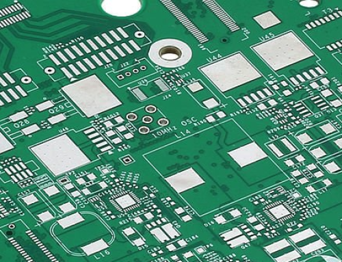
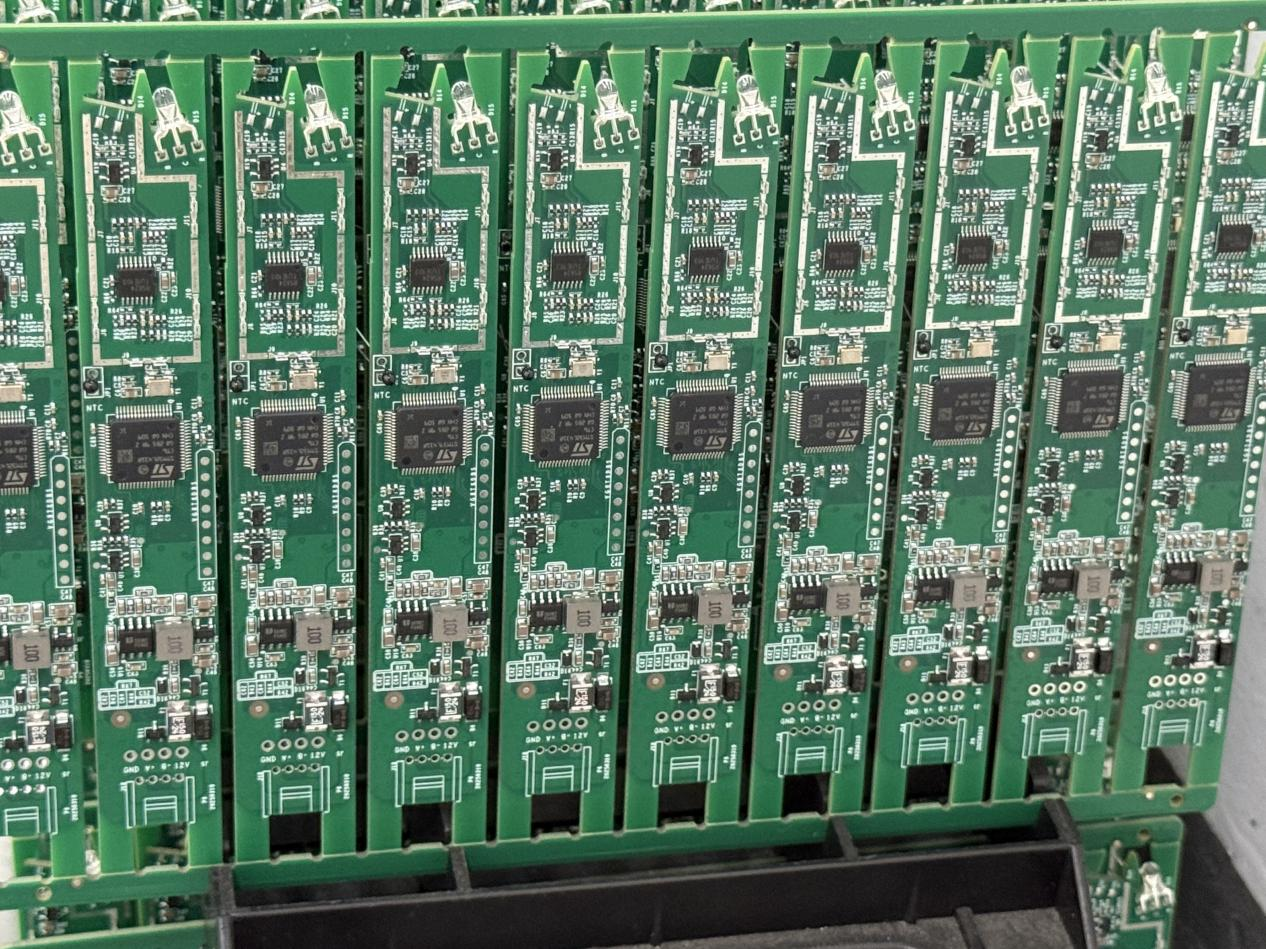
All Shenzhou ALD automatic optical inspection instruments are suitable for lead and lead-free processes.
Third. Responsibilities
1. Operators: general machine operation (on/off, program loading, production testing), daily maintenance
2. Technicians: responsible for program production, adjustment, troubleshooting, monthly maintenance,
and formulation of operating standards.
3. Quality Department: Audit the implementation of operator SOP and equipment maintenance.
Forth. Operation steps
1. Turn the POWER button to ON and turn on the main control computer switch. After the
machine starts, enter the WINDOWS screen, as shown in Figure 1.
2. Click the ALD615 icon on the desktop, enter the user name and password in the dialog
box, or press the confirmation button directly, and the machine will reset, as shown in Figure 2.
3. Load the PCB program to be tested and adjust the width of the guide rail.
4. Insert the PCB in the correct direction, press the LOAD button on the right side of
the machine, and the machine will start automatic inspection, as shown in Figure 3 and Figure 4.

5. After the inspection, the machine displays PASS or a picture of a defective point
that needs to be confirmed. Take out the inspected PCB with your left hand, put another PCB in with your
right hand, and press the LOAD key to automatically inspect the next PCB, as shown in Figure 5.
6. While the machine is automatically inspecting, confirm the previously inspected PCB.
6.1 If the AOI machine inspection shows PASS, no defects are found in the inspection.
The operator marks the specified position of each small piece of PCB and puts it directly into the
electrostatic box in the OK product placement area in order;
6.2 If the machine displays a defective picture, the operator will conduct a second
visual inspection and confirmation of the corresponding components on the PCB (refer to the SMT
appearance inspection standard):
a. If all defective points are confirmed to be AOI misjudgments (false defects) through
visual inspection, the operator marks the specified position of each small piece of PCB and puts it into
the electrostatic box in the OK product placement area in order;
b. If the displayed defective point is confirmed to be NG through visual inspection,
the operator will affix a red arrow label to the corresponding position, put it into the electrostatic
box in the defective product placement area for maintenance, and fill in the AOI inspection daily
report;
c. If there are many defective points detected by AOI or false defects misjudged by
AOI, the technical staff should be notified in time to handle it.
7. Shutdown: After the test is completed, exit the production screen, shut down the
main computer, turn the POWER button to OFF, and turn off the power of the equipment.
Fifth. Precautions:
Shenzhen Highqualitypcb SMT Processing:
1. Anti-static wristbands and anti-static gloves must be worn. When taking or placing
boards, they must be placed horizontally, and they must be placed gently. Do not stack them to prevent
collisions.
2. Good and defective products must be placed separately. After the defective PCB is
repaired, AOI must be re-tested.
3. If there are more than three consecutive abnormalities in the same position, the
technicians must be notified in time to adjust the equipment.

