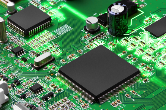
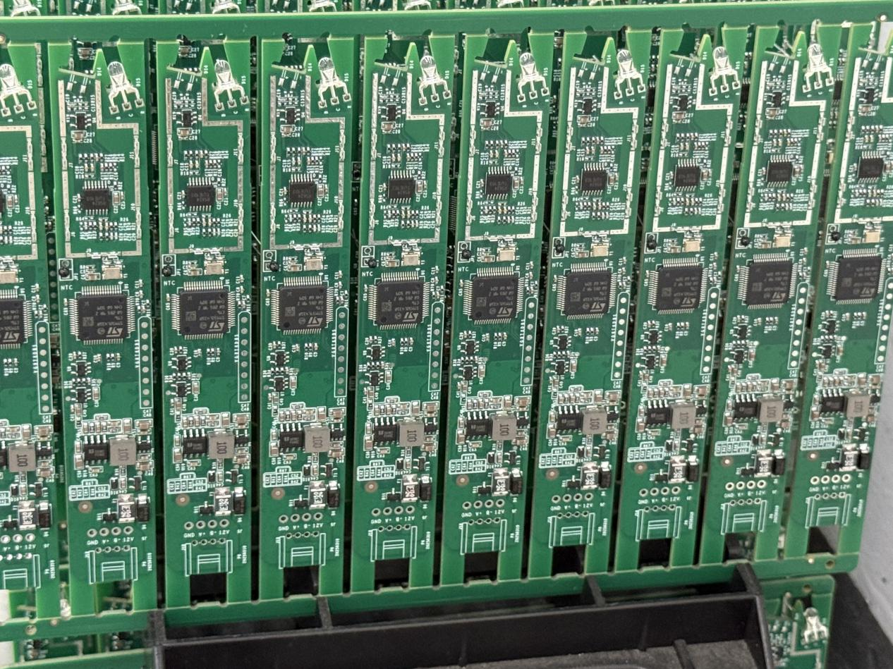
multilayer PCB design introductory tutorial
The article is a beginner's guide to multilayer PCB design, which can help you quickly understand multilayer PCB design.
multilayer PCB design introductory tutorial
If you only lay out a simple one or two-layer circuit board, you will find that laying out a multilayer PCB is similar to a six-layer cake. The cake will take more time, skill, and cost, but it will also be a
happy design challenge without the burden of going to the gym the next day. There will be some new
design methods to learn, and We will introduce these methods to you in our multi-layer PCB design
tutorial.
Step 1 of the Multilayer PCB Design Tutorial: Setup and Preparation
In some cases, an older PCB space may not be large enough for a multi-layer design, so you will need to
determine if there are any additional requirements. Depending on the CAD system used, you may add layers
or attributes to the schematic for multi-layer use. It is where having access to a more advanced PCB
design system with links to online library services. Use the latest and most accurate PCB package source
data to make PCB prototyping easier.
The main difference between two-layer and multi-layer board setups is layer stack up.
Here are some key points to consider when planning your board layer stack up :

Performance: The circuit running speed and the final working environment may influence the materials
used to make circuit boards. There are a variety of higher-grade materials than FR-4, which may be more
suitable for your needs. Still, these materials may affect parameters such as impedance calculations.
The help of PCB manufacturers will be a valuable source of information.
Cost: Manufacturing materials, number of PCB layers, and configuration will directly impact the overall
cost of building circuit board. You need to consider all options with your manufacturer.
Density: The routing density of the board is another factor in determining the PCB layer stack-up
configuration. It is very painful to go back and add layers to your board design after you have already
started the layout. Not only will you need to reconfigure the CAD database, but you may also have to
make many changes to the layout. On the other hand, if you start with too many layers, you will pay more
for your board, so you should do that.
Circuit: You need to understand the demands of the circuit so that you create the best layer
configuration. For example, sensitive signals may require a stripline layer configuration for best
performance, which means adding additional circuit board ground planes. Analog and digital circuit areas
will need to be separated using their ground planes, and the board power supplies will need to be
isolated. These can affect the layer configuration, so this should be planned before the layout begins.
Once the data has been collected and the board layer stack has been created in the layout database, you
can begin placing and routing the board.
Using the Board Outline Generator tool, they create a board layer stack up easily.
Different views on location and route
When working on a multi-layered layout, one of the first things you should consider is the 3D design
aspects. A two-layer board only requires to consider the top and the bottom. But now, you are in a
multi-layer world with many different things happening inside. They can affect the top and bottom. For
example, you may not want to place a noisy part in a certain location because of sensitive routing on
the inner layer below it.
In terms of tools, placing components will be the same as on a double-sided board, but the appearance
used will be different. For example, you won’t have to worry about leaving enough space between parts to
route because they are routed on the internal layers. You’ll still need short, direct paths on surface
layers for sensitive circuits. But, in most instances, you’ll now have more space to work with. It is a
good thing, too, because a multi-layer board might require more components to be placed.
Internal trace routing and power planes will be interesting to work on, but in the meantime, here are
some important considerations:
Multilayer boards typically have more components and routing than double-sided boards. So plan.
Depending on the circuit board technology, some of this routing may have specific routing widths and
spaces or other requirements, such as differential pairs or impedance-controlled routing.
Some routing will require a stripline layer structure and must be routed on a layer near the ground
plane. In addition, sensitive routing must cross vertically on adjacent internal signal layers to help
reduce any possible broadside coupling or crosstalk.
There are many vias holes in the ground plane for connections, but these vias may affect the signal
return path. It requires careful planning of your routes to avoid blocking the signal.
Lay out the split planes so that sensitive signals do not cross the split, disrupting their return path.
Such a situation would generate a lot of noise on the board.
Once you have checked the layout and routing, the remaining design will work similarly to a double-sided
board. Now, you are ready to build the board.
Multi-layer PCB layout requires a 3D perspective for circuit board design.

Complete your design with documentation and output files.
HighQualityPCB Circuit Board Assembly Services: To put a multi-layer PCB design into production, you
need to create the identical documentation you always have, with a few exceptions. First, you will need
more detail on your manufacturing drawings. Your manufacturing drawings will need stackup details for
your multi-layer board, with notes detailing how to build this board. Second, if you are using the
Gerber files for manufacturing output, you need to generate additional files for your multi-layer
boards.
Fortunately, existing PCB design systems already have the tools you need to succeed with multi-layer
board design. CAD PCB Designer is an advanced system that gives you access to an online CAD library
service, a board outline creation wizard, and manufacturing and documentation generation utilities.
