A Complete Guide to HDI PCB
HDI PCB are the tech behind today’s smallest and smartest devices. Here’s how they work, and how to find the right HDI PCB manufacturer for your needs.

Let’s be honest, modern electronics are crammed with more tech than ever, and there’s less room to fit it all. We want thinner phones, smarter wearables, lighter laptops. That’s where HDI PCBs step in.
High Density Interconnect PCBs make all of this possible. You won’t notice them, but they’re everywhere. Inside your smartwatch. Beneath your car’s touch display. Even tucked into medical implants. These boards let engineers build tight, multi-layered circuits with insanely small connections, and still hit performance targets.
So what’s the deal with interconnect PCBs? Why do they matter? And how are they different from regular circuit boards?
We’ll unpack all of that here. If you’re building products, buying from an HDI PCB supplier, or just trying to get your head around what goes on under the hood of advanced devices, this guide was made for you.
1. What Exactly Is an HDI PCB?
Picture a high-rise building in the middle of a crowded city. Every floor is packed with rooms, and every room needs power, plumbing, and Wi-Fi. Now imagine all of that squeezed into a board the size of your hand.
That’s the job of an HDI circuit board.
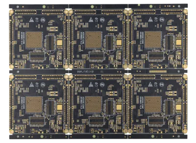
The “HDI” in HDI PCB stands for High Density Interconnect. These boards are built differently from traditional ones. Instead of wide traces and big holes, they use ultra-fine lines, thinner layers, and laser-drilled microvias, those are microscopic holes that connect different layers without taking up much space.
You’ll often hear the term microvia PCB or even microvia PCB when talking about this. The tech behind them is impressive, but the concept is simple: do more, in less space, with better performance.
That’s why HDI printed circuit boards have become standard in industries where real estate is tight and speed is everything. They reduce signal loss, boost routing density, and make devices more reliable overall.
2. Why HDI Tech Powers Modern Devices
Let’s break this down in plain terms. Today’s electronics need to be:
- Small
- Fast
- Durable
- Lightweight
And guess what? HDI boards check all those boxes.
Here’s why so many engineers rely on HDI PCB boards:
- Tighter layouts = smaller devices
Microvias allow for routing in places that standard vias just can’t reach. This lets designers shrink the board without giving up on features.
- Shorter signal paths
Because traces are more direct and layers are stacked more efficiently, signal travel time is reduced. That improves speed and reduces data loss.
- Less weight, more strength
In wearables, satellites, or drones, every gram matters. HDI boards are lighter and often more robust due to better material layering.
- Higher reliability in extreme environments
With fewer mechanical connections and better thermal behavior, HDI PCB electronics manufacturing yields boards that hold up better under stress, ideal for automotive, aerospace, and medical use.
From consumer gadgets to industrial gear, high density interconnect PCBs have made their mark. You’ve probably used half a dozen today without even knowing it.
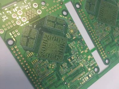
3. The HDI PCB Manufacturing Process
The process behind building an HDI PCB is surprisingly complex. These aren’t just printed boards with extra layers, they’re precision-engineered, laser-drilled, and chemically processed structures designed for tight tolerances.
So, how does an HDI PCB manufacturer actually put one together?
It usually starts with material preparation. Most HDI PCB boards use advanced laminates that can handle high-frequency signals and heat. You need materials that won’t warp, distort, or fail under pressure.
Next up: laser drilling for microvias. Unlike traditional mechanical drilling, this step uses lasers to create microvias, those incredibly tiny, shallow holes that connect copper layers. This is where microvia PCB design shines: small vias mean more routing options and better signal performance.
Then comes layer buildup. Depending on the board’s design (like 1+N+1 or 2+N+2), the manufacturer laminates alternating layers of dielectric material and copper. Each time a layer is added, more vias are drilled, filled, and plated.
This brings us to sequential lamination, a key part of the HDI PCB fabrication process. After each layer is pressed and cured, it’s aligned with the others, often using automated optical positioning to ensure every microvia lands where it should.
Once the buildup is done, manufacturers plate the vias, etch the copper traces, and apply the final surface finish, usually ENIG or OSP. Then comes electrical testing.
And throughout it all? Zero room for error. The HDI PCB manufacturing process demands tight control at every step, because even a slight shift can ruin signal integrity or render layers misaligned.
No wonder HDI PCB fabrication takes longer and costs more. But if your design needs compactness and performance, it’s worth every step.
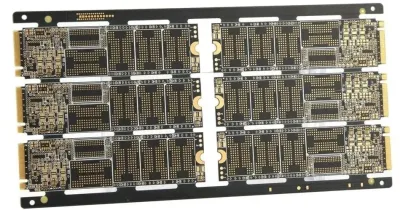
4. Types of High Density Interconnect PCBs (And Why They Matter)
Not all HDI PCBs are created equal. Depending on your layout and performance needs, there are several build-up structures that affect complexity, reliability, and, you guessed it, cost.
Let’s look at the most common types used in HDI PCB electronics manufacturing:
- 1+N+1 HDI PCB
This is your entry-level high density interconnect PCB. It features a core layer with one outer HDI layer on each side. Great for small consumer electronics.
- 2+N+2 HDI PCB
This design adds more HDI layers outside the core, allowing for higher routing density and better via stacking. Think of it as a step up for mobile phones or compact industrial systems.
- ELIC (Every Layer Interconnect)
This one’s serious. ELIC HDI circuit boards allow vias to connect any layer to any other layer. It’s used in high-end computing, aerospace, and complex military hardware.
The more layers and microvias you add, the more precision is required, and the higher the price. That said, the flexibility these designs offer can dramatically reduce footprint while boosting functionality.
This is where working with the right HDI PCB supplier makes a huge difference. Some suppliers specialize in entry-level boards. Others have the capability to deliver multilayer interconnect PCBs with stacked microvias, blind/buried vias, and advanced impedance control.
So before choosing your board structure, ask yourself: how much density do I really need?
5. Benefits and Limitations of High Density Interconnect PCBs
We’ve talked a lot about what HDI PCBs do. But what are their real-world pros and cons?
Let’s break it down:
5.1 Benefits
- Space-Saving Design
This is the #1 reason designers go with HDI printed circuit boards. Smaller boards mean smaller products, and HDI makes that possible.
- Better Performance at High Frequencies
With shorter signal paths and optimized routing, high density interconnect PCBs reduce noise and signal loss, especially important in high-speed applications.
- Fewer Layers, More Function
A well-designed hdi pcb board can replace a bulkier multilayer PCB, reducing not just size but overall complexity.
- Stronger Reliability
Fewer through-holes, more solid connections. That leads to longer-lasting boards in harsh conditions.
5.2 Limitations
- Higher HDI PCB Cost
No sugar-coating it, HDI PCB fabrication is more expensive than traditional boards. Laser drilling, multiple lamination cycles, and tight quality control all add up.
- Complex Manufacturing
You need a trusted HDI PCB manufacturer. Not every board shop can handle microvias, stacked layers, or advanced finishes.
- Difficult Prototyping
The same precision that makes HDI PCBs amazing also makes them hard to prototype in small runs.
Still, the benefits often outweigh the limitations, especially if your product lives or dies by form factor, speed, or durability.
6. What Actually Affects HDI PCB Cost?
Let’s talk numbers, because HDI PCBs aren’t cheap, and there’s a good reason for that.
You’re not just paying for a circuit board. You’re paying for precision. For microvias. For layered structures that need to survive inside smartphones, satellites, and surgical equipment.
Here’s what influences HDI PCB cost:
6.1 Layer Count
The more layers your hdi pcb board has, the more build-up cycles it needs. Every added layer means more lamination, more alignment steps, more time.
6.2 Via Structures (Blind, Buried, Microvia)
Using stacked microvias or complex via-in-pad structures requires extra drilling, plating, and inspection. This is where microvia PCB builds start to push up cost.
6.3 Material Selection
Need high-speed signal performance or special thermal properties? Premium laminates cost more, but they’re essential for HDI PCB electronics manufacturing in 5G, aerospace, or automotive applications.
6.4 Surface Finish Type
ENIG, OSP, immersion silver, hard gold… each finish has pros, cons, and pricing differences. Higher-end finishes = better solderability and durability = more dollars.
6.5 Order Volume
Prototypes and small runs are expensive. If you can scale up to a production batch, most HDI PCB suppliers will cut the per-unit price significantly.
Pro Tip: To keep HDI PCB fabrication affordable, don’t over-specify. Collaborate early with your HDI PCB manufacturer to simplify the stack-up, optimise materials, and avoid unnecessary blind vias.
7. How to Pick the Right HDI PCB Manufacturer (Without Regret)
Choosing an HDI PCB manufacturer isn’t like ordering stickers online. The stakes are higher. One mistake, and your boards don’t just arrive late, they arrive useless.
Here’s how to find someone who knows what they’re doing.
1) Look for microvia experience
Ask if they’ve built microvia PCBs before, and how often. A serious manufacturer will walk you through drill tolerances, fill types, and reliability testing.
2) Ask about certifications
RoHS, ISO 9001, UL, any legit HDI PCB supplier should have documentation ready. No certifications? That’s your cue to run.
3) Engineering support
The best suppliers don’t just print your files, they check them. They ask about your end-use case. They’ll flag issues before they hit production.
4) Watch out for red flags
- Generic replies
- No stack-up suggestions
- No impedance control experience
- Limited testing capabilities
If a high density interconnect PCB is your core product, don’t gamble with a cheap quote. Work with a manufacturer who gets it right the first time.
8. HDI PCB Design Tips from Real-World Builds
Designing an HDI PCB isn’t just about cramming components onto a tiny board. It’s about balance, performance, reliability, and manufacturability.
Here’s what to keep in mind:
- Avoid vias in tight clusters
Give microvias room to breathe. Dense via farms might look clever but can cause signal issues and delamination during lamination.
- Mind your signal paths
For high-speed designs, trace length matters. Use HDI PCB manufacturing process guidelines to keep impedance stable across layers.
- Watch component placement near edges
In tight layouts, it’s tempting to push chips to the board’s edge. But that increases stress during reflow and handling. Keep a buffer zone.
- Stack with purpose
Don’t just add layers because you can. Every extra layer adds time, cost, and complexity. Start with a realistic interconnect PCB layout, then add only what you need.
- Ask for a DFM review early
Great HDI designs are born from teamwork. Your HDI PCB supplier should help you tweak the design before it hits the production floor.
9. What’s Next for High Density Interconnect PCB Technology?
HDI PCBs aren’t new, but they’re evolving fast.
Here’s where things are heading:
1) AI-Driven PCB Layouts
With AI assisting in board routing and stack-up planning, engineers can now create HDI PCB layouts that optimise for performance and cost in real-time.
2) Hybrid Builds with Flex Layers
We’re seeing more projects combine HDI PCB boards with flexible layers, especially in wearables and foldable tech. Think: curved displays, smart bands, compact sensors.
3) Automotive and Aerospace Growth
Vehicles are now packed with microcontrollers and sensors. That means more demand for high density interconnect PCBs that can handle vibration, heat, and space limits.
4) Smaller Packages, Higher Layer Counts
As components shrink, the layer count goes up. Expect to see ELIC designs and 6+ layer HDI stacks becoming the norm in consumer tech.
5) Medical and Implantable Devices
From neural interfaces to micro-monitoring tools, HDI PCB electronics manufacturing is being pushed to its limits for ultra-thin, biocompatible, multi-function boards.
10. High Density Interconnect PCB FAQs
11. Summary
Why HDI PCBs are the backbone of modern tech? Let’s wrap this up.
HDI PCBs make modern electronics possible. They’re built smaller, faster, and smarter than traditional boards, thanks to microvias, stacked layers, and high-density routing.
If you’re building a product that needs compact power, faster signal transmission, or just more features in less space, high density interconnect PCBs aren’t optional, they’re essential.
From understanding the HDI PCB manufacturing process, to picking the right HDI PCB supplier, to designing boards that are fast, reliable, and affordable, every decision matters.
So, whether you’re an engineer, a buyer, or a curious builder, remember this: the future of hardware is dense. And interconnect PCBs are how we build it.
related Posts

Contact us
WhatsApp: +86-18123905375
Wechat: +86-18123905375
Skype: ali_youte
Email: sales@highqualitypcb.com