A Guide to PCB Assembly Process in 2025
2025 PCB assembly guide: Covers SMT/through-hole processes, inspection methods, rework techniques & testing for DIY & professional production.

Electronics have become an integral part of our daily lives. PCBs are an important component. When you see these smart gadgets, have you ever wanted to create your own electronic devices? The urge to create something unique is common. But without proper guidance, even simple projects can go wrong.
This article offers a detailed, step-by-step manual for PCB Assembly by hand. It covers everything from preparation to assembly, testing, and troubleshooting. It is also suitable for both small-batch prototypes and DIY enthusiasts. Follow these 5 core steps, and you’ll boost your project’s success rate by 95%.
1.What is PCB Assembly?
PCB assembly refers to the process of attaching electronic components to a circuit board. PCBAs (Printed Circuit Board Assemblies) are critical for creating complex electronic systems. It is also important to develop devices for targeted applications. PCB assembly can be done manually or through automated processes. Due to advancements in robotic technology, automated methods have gained significant popularity in recent years. That said, certain steps often remain manual, particularly for specialized or custom PCB designs.
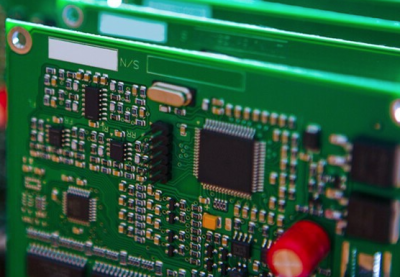
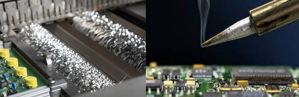
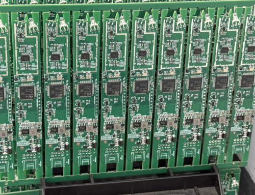
PCB Assembly
2.Pre-assembly Prepared
2.1 Tools and Materials
(1)Tools Required:
Essential Solder Tools: Soldering iron, Solder, Flux.
Auxiliary Tools: Tweezers, Diagonal cutters, Wick/pump, Multimeter, PCB clamp/holder, Anti-static wristband, Magnifying glasses or microscopes (optional, for small SMT parts).
(2)Materials:
Blank PCB (with copper trace and predrilled holes).
Electronic components (resistors, capacitors, ICs, connectors, etc.).
Solder paste for SMT parts (if reflow soldering is used).
Cotton swabs with isopropyl Alcohol for cleaning flux residue
2.2 PCB Layout and Preparation
(1)PCB Inspection:
Visual Check: Examine the board for physical defects (e.g., cracks, misdrilled holes).
Electrical Testing: Use a multimeter to verify trace continuity and identify open circuits.
Insulation Test: Measure resistance between adjacent traces to ensure no unintended conductivity.
(2)PCB Cleaning:
Contamination Removal: Wipe pads with isopropyl alcohol (IPA) to eliminate oil, fingerprints, or dust. For stubborn flux residue, use ultrasonic cleaning with a neutral detergent.
Pad Pre-Treatment: Remove the oxidation and protect the solder mask.
(3)Positioning and Marking:
- Fiducial Marks:
SMT Alignment: As a pick-and-place machine alignment, add 3 copper marks on the PCB edge.
Manual Setup: Draw crosshairs on corner edges with a permanent marker. And align them with workbench grid paper for consistent component orientation.
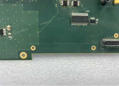
Fiducial Marks
- Specialized Pad Preparation:
BGA Pads: Use a magnifying lens to check the flatness of the pad. Reject boards with large depressions in order not to create solder bridges.
Oxidized Pads: Gently sand and reactivate with flux using a soldering iron.
Damaged Pads (>30% copper loss): Bridge with jumper wires or adjacent vias to restore continuity.
Through-Hole Deburring: Use a reamer to smooth hole edges and ensure easy lead insertion. Match hole diameter to component leads (avoid loose fit or excessive insertion force).
(4)SMT-Specific Cleaning:
Wipe SMT pads with IPA-dipped swabs to remove oils.
Treat grayish pads with flux to improve solder wettability.
2.3 Component Layout and Preprocessing
(1)Design Review:
Cross-verify component footprints against schematics, ensuring no missing test points or redundant features.
Confirm correct placement, polarity, and orientation for polarized components (diodes, capacitors).
(2)Component Preparation:
- THT Components:
Remove lead oxidation with sandpaper or a wire brush.
Bend leads to match PCB holes using pliers, adjusting spacing as needed.
- SMT Components:
Inspect terminals under a magnifier; clean oxidized parts with ethanol.
Handle with anti-static tweezers to avoid ESD damage (wear an ESD wrist strap).
For QFP/SOP ICs, check lead coplanarity and use a leveling tool if misaligned to prevent cold joints.
3.Surface-Mount Technology (SMT) Assembly
Surface-Mount Technology (SMT) Assembly
3.1 Hand Soldering (Low-Volume Use)
(1)Flux Application: Apply a small dab of flux (if not using flux-cored solder) to improve pad wetting.
(2)Component Placement: Use tweezers to align component pins precisely with PCB pads.
(3)Tack Soldering: Secure the component by soldering one corner pin first. Then check alignment and adjust if needed.
(4)Full Soldering: For SOIC/QFP ICs, gently drag the soldering iron along the pins, feeding the solder as required. For 0603/0805 components, solder one pad, place the part, and then solder the second pad.
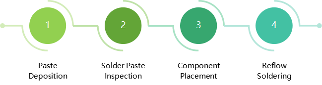
3.2 Solder Paste + Reflow (Mass Production)
(1)Paste Deposition: Use stencils and a squeegee to apply solder paste evenly onto pads.
(2)Solder Paste Inspection (SPI):
2D SPI: Measures paste height and width to ensure proper coverage.
3D SPI: Analyzes paste volume, length, and width, detecting issues like insufficient or misplaced solder.
(3)Component Placement: Use a pick-and-place machine or tweezers to position components on the paste.
(4)Reflow Soldering: Reflow soldering is conducted only for SMT assembly. Wave soldering for through-hole components will be discussed later. The circuit board and the components are placed in the reflow oven. The solder paste melts in this stage. Upon cooling, it creates a solid bond between the component and its pads. The components are fixed rigidly to the board.
Temperature ranges for reflow soldering depend on the type of solder paste. Lead solder paste should be heated to 180-220degc and lead-free paste at 210-250degc.
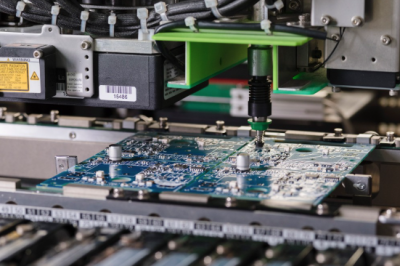
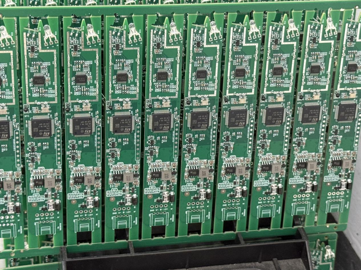
Assembly Process
3.3 Automated Optical Inspection (AOI)
AOI systems use cameras and sensors to examine PCB solder joints and component orientation. They identify many defects. These defects include missing parts, misaligned components, incorrect polarity, solder bridges, insufficient solder, and open circuits. We use them to ensure quality control.
3.4 X-Ray Inspection
X-ray inspection is a non-destructive testing (NDT) method. The images reveal the internal structures of complex multilayer PCBs with fine-pitch components. It detects hidden solder joint defects, such as voids or cold joints, in hard-to-reach areas.
3.5 Flying Probe Testing (FPT)
FPT is an automated testing method. It uses movable probes (adjustable in XYZ axes) to identify open circuits and shorts. It can also measure component values (resistance, capacitance, inductance). It is ideal for small batches or frequent design changes. It uses netlist data from design files to test electrical properties by probing various points on the PCB.
The SMT assembly is complete. Through-hole components will be examined to determine if they are non-washable. If they are present, the same as surface-mounted components that cannot be washed, these are kept aside and soldered once cleaned.
4.Through-Hole Component Assembly
- Wave Soldering: Place components on a PCB and apply liquid flux to lead terminals. Then preheat the board to a precise temperature. Lastly, pass it over a moving solder wave via a conveyor belt to form joints. It is ideal for mass production.
- Hand Soldering: Mount components on a PCB using soldering tools and wire solder. Apply flux to clean metal surfaces. We should combat oxidation during the soldering process. It ensures reliable connections.
Wave Soldering vs Hand Soldering
- Selective Soldering: Apply solder to specific through-hole components on a PCB. We use robotic soldering systems or specialized nozzles to achieve it. The equipment includes flux spray, a solder pot, and a moveable solder head. It offers faster, more consistent results than manual soldering for targeted connections.
4.1 Component Insertion
(1)Install Small Components First: Begin with resistors and small capacitors. This can avoid obstructing adjacent pads.
(2)Align Pins: Insert component leads through PCB holes from the top (component side). This can ensure a 1–2mm protrusion on the solder side.
(3)Secure Tall Components: We can use clamps or temporary fixtures for connectors/transformers. This prevents movement during soldering.
(4)Check Polarity: Verify correct orientation (e.g., diodes, electrolytic capacitors). This can avoid damage from reverse installation.
4.2 Soldering
(1)Preheat the Pad: Touch the soldering iron tip (angled at 45°) to both the pad and lead until the pad darkens slightly.
(2)Apply Solder: Feed the solder into the joint (not the iron) until a smooth fillet forms. Avoid excess solder.
(3)Remove Iron: Allow 1 second for solidification before moving the board.
4.3 Lead Trimming
(1)Trim Excess Leads: Use flush-cut pliers to trim leads, leaving 1mm to prevent pad lifting.
(2)ESD Control: Immediately remove trimmings with a sticky pad or compressed air. This prevents short circuits.
5.Inspection and Rework
5.1 Inspection
(1)Visual Inspection
| Inspection Item | Acceptance Criteria | Common Defects and Identification |
| Solder Joint | Smooth, no bridge | Cold joints (dull surface), bridges, insufficient solder |
| Component | Correct polarity, aligned | Missing parts, reserved ICs, BOM mismatches |
| Pads/Traces | No delamination; ≥0.1mm spacing | Damaged pads (>30% copper loss ), trace shorts |
| Flux Residue | No sticky white/yellow deposits | Excessive residue (risk of corrosion) |
Continuity Test: Use a multimeter to verify connections between leads and pads. It checks for shorts/opens.
5.2 Rework
(1)Component Replacement:
- Through-Hole: Use a desoldering wick or a pump to remove solder. Gently lift the component while heating.
- SMT: Apply heat with a rework station. Lift with tweezers once the solder melts. Then reapply paste and solder.
(2)Pad Repair:
- Minor Damage (<50% Copper Loss): Clean the area, apply flux, and bridge with enameled wire secured by high-temperature tape.
- Complete Pad Loss: Solder directly to the exposed inner layer via, ensuring connectivity.
(3)Defects:
- THT Defects:
Solder Bridges: Apply flux, place desoldering wick, and heat to absorb excess solder.
Cold Joints: Add flux and reflow solder until smooth.
- SMT Defects:
Misalignment: Use hot air to melt solder, and realign with tweezers.
QFP Bridges: Use a fine-tip iron to separate joints via surface tension. Remove excess solder with a wick first if needed.
5.3 Post-Rework Steps
- Clean Residue: Wipe the area with isopropyl alcohol to remove flux and debris. It can prevent corrosion.
- Reinspect: Visually check repairs, retest continuity, and verify IC functionality.
6.Cleaning, Testing, and Final Debugging
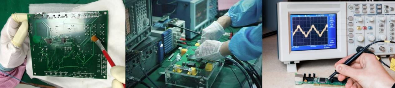
Cleaning, Testing, and Final Debugging
6.1 Cleaning
(1)Purpose: Prevent corrosion, signal interference, and poor conformal coating adhesion.
(2)Manual Steps:
- Apply isopropyl alcohol (IPA) to contaminated areas.
- Gently scrub with a brush or swab.
- Dry with compressed air or a lint-free cloth.
- Inspect under UV light to detect residual flux.
Cautions: Avoid acetone on plastics/silkscreens. Use ESD-safe tools for sensitive components.
6.2 Testing
(1)Pre-Power Safety Check:
Short Detection: Measure resistance between VCC and ground. If low, check for reversed capacitors, bridged IC pins, or exposed traces.
Continuity Test: Randomly test 10% of components (prioritize SMT parts) using a multimeter’s continuity mode.
(2)Automated Optical Inspection (AOI):
Industrial: High-resolution cameras compare PCBs to CAD models for missing/misaligned components.
DIY Alternative: Use open-source software with a USB microscope for basic pattern recognition.
(3)X-ray Inspection: Detect hidden BGA/QFN defects (e.g., solder voids, insufficient underfill).
(4)Functional Testing: Power the board. Validate component values (resistance, capacitance) and signal paths.
6.3 Debugging
(1)Common Failures:
Power Issues: Check regulators, diode orientation, and fuse continuity for no power/voltage drops.
Signal Integrity: Add decoupling capacitors or reroute noisy traces to fix glitches/EMI.
Firmware/Software: Review code/logs. Or use JTAG debuggers for MCU freezes or communication errors.
(2)Debugging Process:
- Isolate Problems: Test functional blocks (power, analog, digital) separately.
- Trace Signals: Use an oscilloscope to follow signals from input to output.
- Component Checks: Replace suspected faulty parts (e.g., swap ICs).
- Environmental Testing: Validate performance under temperature/vibration stress.
7.PCB Assembly FAQs
8.Summary
PCB assembly transforms circuit designs into functional electronics through a meticulous process. Every step—from design verification to testing—is critical for quality. Mastery of these skills is essential for professionals working on electronic prototypes or high-volume production in today’s tech-driven landscape.
