How to complete PCBA within 1 hour – quick turn PCB assembly
This article introduces the PCBA process in detail.
Table of Content
How to complete PCBA within 1 hour – quick turn PCB assembly

PCBA
Printed circuit board assembly is one of the crucial steps in electronic manufacturing. Yet, it’s also
vital to shorten the time cycle while ensuring quality.
So, how do you achieve fast turnaround PCB assembly? Highqualitypcb is one of the fast-turnaround
printed circuit board manufacturers. It has highly automated and efficient production lines. They can
accomplish this task.
This article introduces the brief PCBA process in detail. Each step is optimized to ensure the completion of the process in a short time.
Design preparation (5 minutes)
Before production, the design team must complete circuit schematics, PCB layout design, and component
packaging.
First, the design team needs to design the circuit. It includes making circuit diagrams, printed circuit
board layouts, and defining component packages.
The circuit schematic is the blueprint of the circuit, which clarifies the connection between components
and the signal transmission path. The PCB layout design determines the layout of electronic components
on the circuit board. It ensures the correct position and wiring of the components to realize the
function of the circuit.
The challenge at this stage is that designers must complete complex design work in a short, so it
requires efficient workflows and tools. When designing the circuit diagram, one needs to consider a few
factors, such as circuit performance, maintainability, thermal management, and impedance control. It
ensures that the printed circuit board assembly can meet the specification requirements.
Material preparation (5 minutes)
Prepare the required raw materials, including circuit board, components, pads, connectors, and welding
materials. Supply chain management and inventory control are crucial to ensuring a timely supply of
materials.
During the material preparation phase, the supply chain team must work closely to ensure all required
materials are ready to meet production needs.
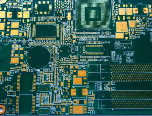
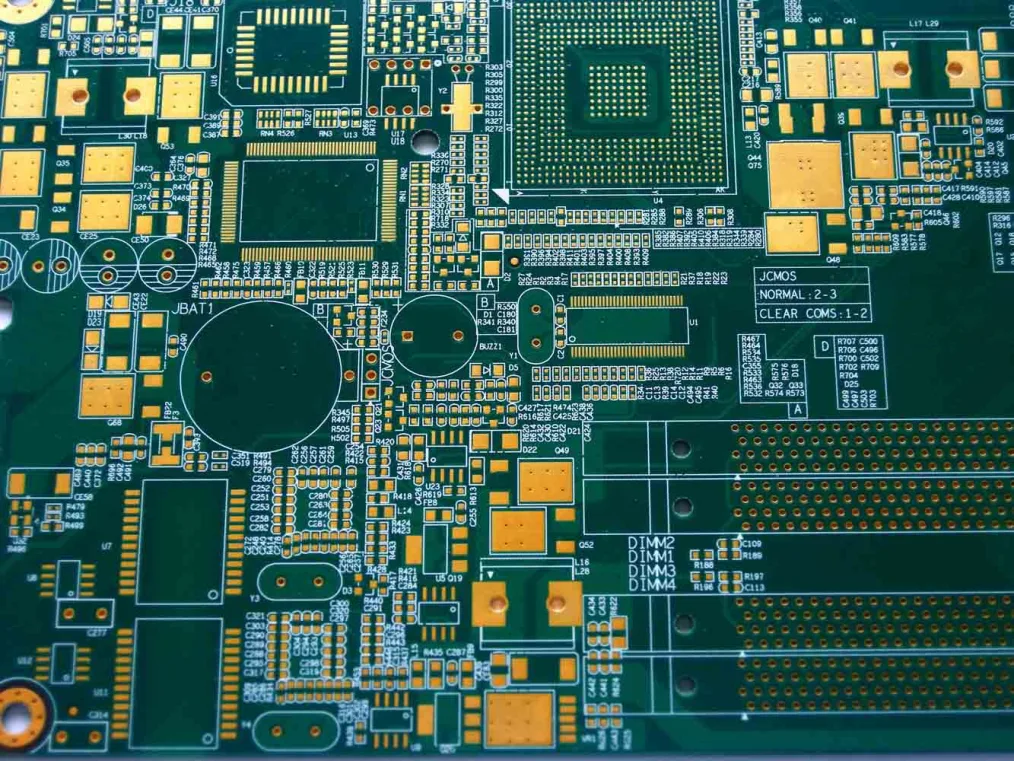
PCB manufacturing (10 minutes)
The circuit pattern is printed onto the circuit board using a high-speed printer, and A CNC drilling
machine drills the holes. This step requires high precision and automation to speed up production.
1) Print circuit board
Use a high-speed printer to print the circuit pattern onto the PCB board, ensuring production efficiency.

high-speed printer
2) Drilling
Use a CNC drilling machine to drill holes. The CNC drilling machine ensures the correct installation or
connection of components by controlling the accuracy of drilling.
They are usually automated. They can operate at speeds and perform precise operations. They do this
according to predetermined design requirements.
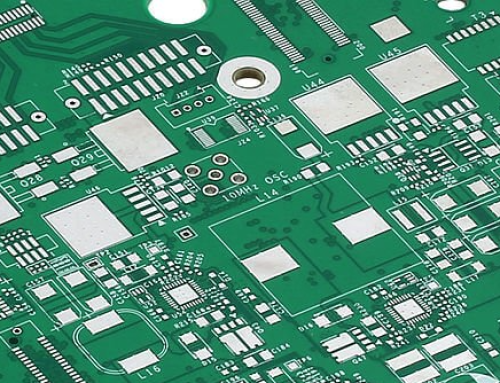
3) Quality management
Automatic optical inspection equipment ( AOI, X-ray ) detects printing or drilling problems in
real-time. They ensure each PCB meets quality standards.

inspection equipment
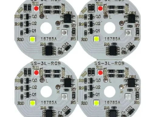
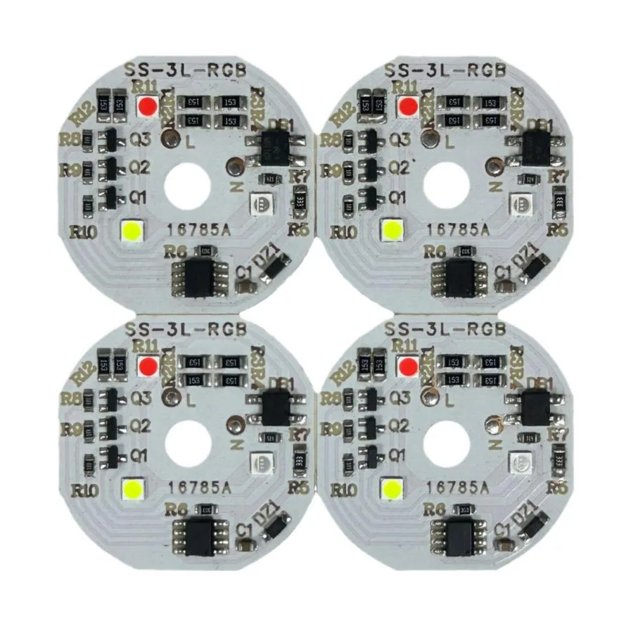
SMT assembly (15 minutes)
Use an automatic placement machine to quickly and accurately paste the components onto the PCB board.
And then pass them through a reflow oven for soldering.
This step needs much automation and precise control. It ensures that components are correctly mounted
and soldered on the PCB.
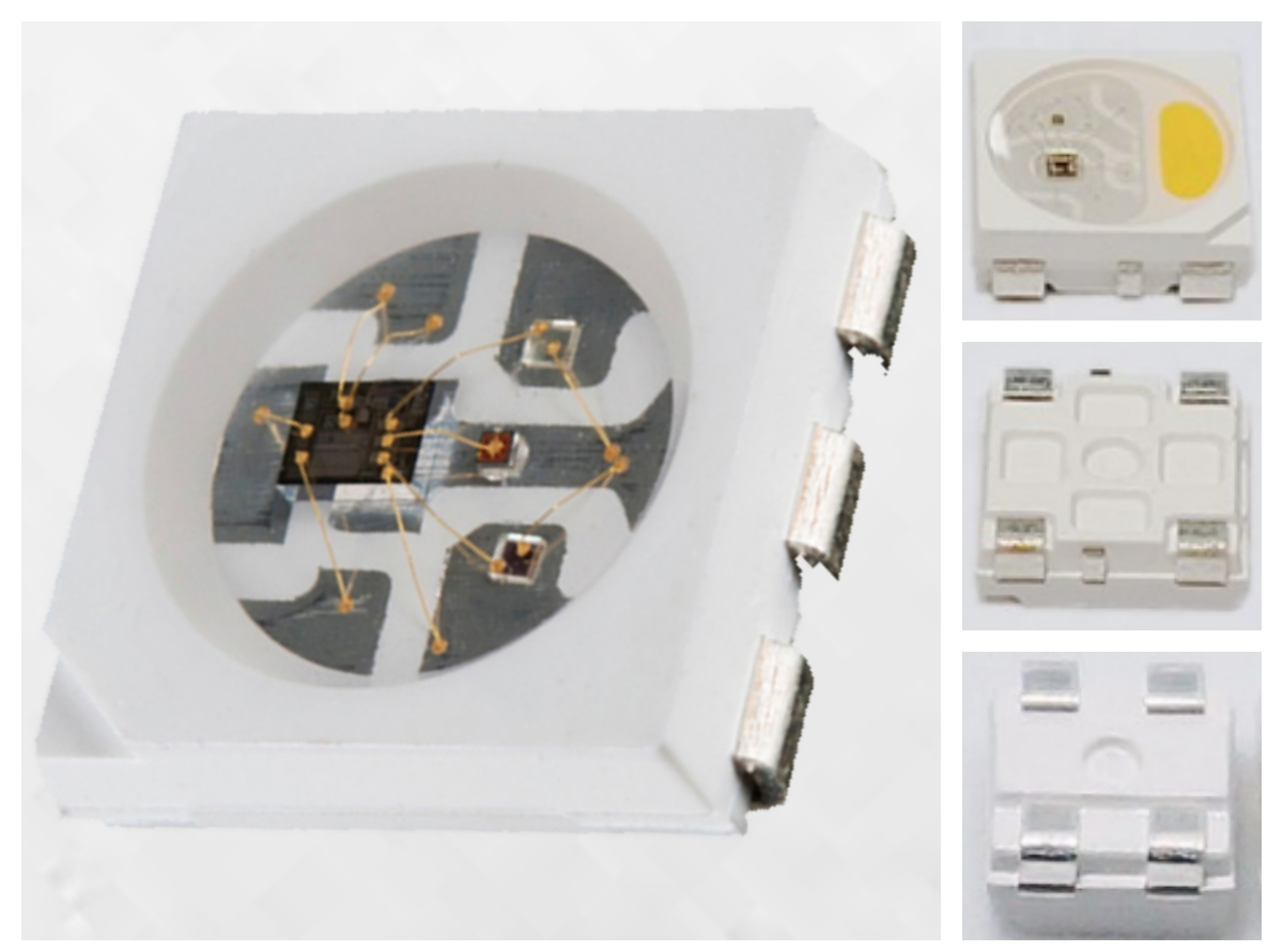
1) Surface mount
Automatic placement machines can quickly and accurately select, position, and paste components onto
circuit boards. These machines can handle a large number of components, improving production efficiency.
Vision systems can detect the correct position of components to ensure accurate placement on the PCB.

Surface mount
2) Welding
The soldering stage usually uses a reflow oven.
A reflow oven is a device that precisely controls temperature and heat, which melts solder paste on
component leads and pads to form a solid solder connection.
During the welding process, temperature and time control are crucial to ensure the welding quality. A
highly automated welding process can ensure consistent welding quality and reduce the risk of human
error.
This step requires diversity in component packaging. Different components have different sizes, shapes,
and pin arrangements.
Also, soldering must consider the PCB’s characteristics. These include the size and shape of the pads
and the presence of the solder mask.

reflow oven
3) Quality inspection
We use automated optical inspection equipment to check the position of components and soldering quality.
PCBA inspection and repair (5 minutes)
We use automated optical inspection equipment to check solder joint quality and component position. If a
problem is found, the repair system can fix it. Or it can flag the problem for manual fixing.

manual fixing
Printed circuit board assembly test (10 minutes)
Place the assembled PCBA into the test equipment for electrical testing, functional testing, and
performance testing.
The automatic test bench can perform multiple tests simultaneously to improve efficiency.
PCBA Packaging and Marking (5 minutes)
Put the tested PCBAs into anti-static bags and mark them for easy tracking and differentiation. It helps
reduce the time for subsequent logistics and distribution.
Final inspection and quality control (5 minutes)
A final quality check ensures that each printed circuit board assembly meets quality standards. This
includes visual inspection and electrical parameter verification.
Packing and shipping (5 minutes)
The team packages the printed circuit board assembly into a final product and prepares the shipping
paperwork. The product can be stored in inventory waiting for distribution or shipped immediately.
Summary
The above processes emphasize high automation, precise control, and close coordination to ensure
completing the PCB assembly process within one hour.
Different PCBAs and products may require different process flows, but high efficiency and quality
control are crucial factors.
related Posts

Contact us
WhatsApp: +86-18123905375
Wechat: +86-18123905375
Skype: ali_youte
Email: sales@highqualitypcb.com